Search results with tag "Snubber circuits"

Application note Snubber Circuits Table of contents
www.hiquel.comApplication note Snubber circuits for inductive loads HIQUEL GmbH, Bairisch Kölldorf 266, A-8344 Bad Gleichenberg, AUSTRIA, Tel: +43-(0)3159-3001, Fax: +43-(0)3159 ...

Designing Flyback Converters Using Peak-Current-Mode ...
pdfserv.maximintegrated.comSnubber circuits are used to limit the voltage overshoots to safe levels within the voltage rating of the external MOSFET. The snubber capacitor can be calculated using the following equation: (Eq. 9) 3DJH RI Where LLK is the leakage inductance that can be obtained from the transformer specifications (usually
Snubber Circuit for Buck Converter IC : Power Management
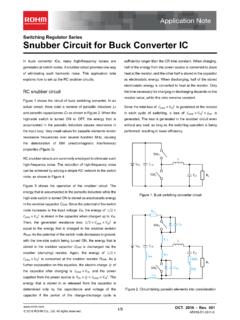
fscdn.rohm.comSnubber Circuit for Buck Converter IC In buck converter ICs, many high-frequency noises are generated at switch nodes. A snubber circuit provides one way of eliminating such harmonic noise. This application note explains how to set up the RC snubber circuits. RC snubber circuit Figure 1 shows the circuit of buck switching converter. In an

RC snubber circuit design for TRIACs - STMicroelectronics
www.st.comSnubber circuit functions and drawback AN437 4/18 Figure 4. Z0103 TRIAC turn-off on inductive load without and with snubber circuit (C = 10 nF and R = 2.7 kΩ) The snubber circuit design, detailed in Section 2: How to design snubber circuit for turn-off improvement, is a trade-off between the maximum peak off-state voltage under pulse conditions (VDSM / VRSM), the …
Snubber Circuits: Theory , Design and Application
www.ti.comthe parasitic resonances in the power stage and is probably the most widely used of all snubber circuits. It is used on output inductors and the secondaries of transformers as well as across diodes and switches. It is applicable both to rate of rise control and to …
Snubber Circuits Suppress Voltage Transient Spikes in ...
pdfserv.maximintegrated.comSnubber Circuits Suppress Voltage Transient Spikes in Multiple Output DC-DC Flyback Converter Power Supplies Nov 12, 2001 Abstract: The flyback dc-dc converter topology results in significant cost and space savings for multiple output power supplies with high output voltage for power levels up to 100W. Flyback topologies store

Reducing noise on the output of a switching regulator
www.ti.comSnubber circuit A snubber circuit contains a resistor and capacitor that should dampen the switch-node ringing by absorbing the energy stored in the parasitic elements of the MOSFETs and printed circuit board (PCB). For more detail about designing a snubber circuit, see Reference 2. The test board used a 330-pF C SNUB and an 8.2-Ω R SNUB.

Chapter 5 Protection Circuit Design - Fuji Electric
www.fujielectric.comSnubber circuit schematic Circuit features (comments) Main application C snubber circuit • This is the simplest circuit • The LC resonance circuit, which consists of a main circuit inductance coil and snubber capacitor, may cause the C-E voltage to oscillate.
Topologies for switch mode power supplies
www.st.comthe circuit capacitance and the primary to secondary transformer leakage inductance. So, a single switch flyback nearly always requires a snubber circuit limiting this voltage spike (see figure 5). In a double switch flyback, the leakage inductance of the power transformer is much less critical (see figure 6). The two demagnetization diodes (D ...