Transcription of TL084, TL084CN GENERAL PURPOSE QUAD JFET OP …
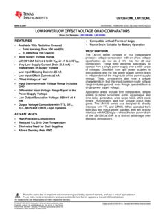
1 TL084. TL084A - TL084B. GENERAL PURPOSE J-FET. quad OPERATIONAL AMPLIFIERS. WIDE COMMON-MODE (UP TO VCC+) AND. DIFFERENTIAL VOLTAGE RANGE. LOW INPUT BIAS AND OFFSET CURRENT. OUTPUT SHORT-CIRCUIT PROTECTION. N. HIGH INPUT IMPEDANCE J FET INPUT DIP14. STAGE (Plastic Package). INTERNAL FREQUENCY COMPENSATION. LATCH UP FREE OPERATION. HIGH SLEW RATE : 16V/ s (typ) D. SO14. (Plastic Micropackage). p TSSOP14. (Thin Shrink Small Outline Package). ORDER CODE. DESCRIPTION Package Temperature Part Number Range The TL084, TL084A and TL084B are high speed N D P.
2 J FET input quad operational amplifiers incorpo- TL084M/AM/BM -55 C, +125 C . rating well matched, high voltage J FET and bipo- TL084I/AI/BI -40 C, +105 C . lar transistors in a monolithic integrated circuit. TL084C/AC/BC 0 C, +70 C . Example : TL084CN , TL084CD. The devices feature high slew rates, low input bias N = Dual in Line Package (DIP). and offset currents, and low offset voltage temper- D = Small Outline Package (SO) - also available in Tape & Reel (DT). P = Thin Shrink Small Outline Package (TSSOP) - only available ature coefficient.
3 In Tape & Reel (PT). PIN CONNECTIONS (top view). Output 1 1 14 Output 4. Inverting Input 1 2 - - 13 Inverting Input 4. Non-inverting Input 1 3 + + 12 Non-inverting Input 4. VCC + 4 11 VCC - Non-inverting Input 2 5 + + 10 Non-inverting Input 3. Inverting Input 2 6 - - 9 Inverting Input 3. Output 2 7 8 Output 3. March 2001 1/12. TL084 - TL084A - TL084B. SCHEMATIC DIAGRAM (each amplifier). VCC. Non-inverting input Inverting input 1 0 0 . 2 0 0 . Output 1 0 0 . 30k 35k 35k 1 0 0 . VCC. ABSOLUTE MAXIMUM RATINGS.
4 Symbol Parameter TL084M, AM, BM TL084I, AI, BI TL084C, AC, BC Unit VCC Supply voltage - note 1) 18 V. Vi Input Voltage - note 2) 15 V. Vid 3) 30 V. Differential Input Voltage - note Ptot Power Dissipation 680 mW. Output Short-circuit Duration - note 4) Infinite Toper Operating Free-air Temperature Range -55 to +125 -40 to +105 0 to +70 C. Tstg Storage Temperature Range -65 to +150 C. 1. All voltage values, except differential voltage, are with respect to the zero reference level (ground) of the supply voltages where the zero reference level is the midpoint between VCC + and VCC.
5 2. The magnitude of the input voltage must never exceed the magnitude of the supply voltage or 15 volts, whichever is less. 3. Differential voltages are the non-inverting input terminal with respect to the inverting input terminal. 4. The output may be shorted to ground or to either supply. Temperature and/or supply voltages must be limited to ensure that the dissipation rating is not exceeded 2/12. TL084 - TL084A - TL084B. ELECTRICAL CHARACTERISTICS. VCC = 15V, Tamb = +25 C (unless otherwise specified).
6 TL084I,M,AC,AI,AM, TL084C. Symbol Parameter BC,BI,BM Unit Min. Typ. Max. Min. Typ. Max. Input Offset Voltage (Rs = 50 ) mV. Tamb = +25 C TL084 3 10 3 10. TL084A 3 6. Vio TL084B 1 3. Tmin Tamb Tmax TL084 13 13. TL084A 7. TL084B 5. DVio Input Offset Voltage Drift 10 10 V/ C. Input Offset Current - note 1). Iio Tamb = +25 C 5 100 5 100 pA. Tmin Tamb Tmax 4 4 nA. Input Bias Current -note 1. Iib Tamb = +25 C 20 200 20 400 pA. Tmin Tamb Tmax 20 20 nA. Large Signal Voltage Gain (RL = 2k , Vo = 10V) V/mV.
7 Avd Tamb = +25 C 50 200 25 200. Tmin Tamb Tmax 25 15. Supply Voltage Rejection Ratio (RS = 50 ) dB. SVR Tamb = +25 C 80 86 70 86. Tmin Tamb Tmax 80 70. Supply Current, no load, per amplifier mA. ICC Tamb = +25 C Tmin Tamb Tmax Vicm 11 +15 11 +15 V. Input Common Mode Voltage Range -12 -12. Common Mode Rejection Ratio (RS = 50 ) dB. CMR Tamb = +25 C 80 86 70 86. Tmin Tamb Tmax 80 70. Output Short-circuit Current mA. Ios Tamb = +25 C 10 40 60 10 40 60. Tmin Tamb Tmax 10 60 10 60. Output Voltage Swing V.
8 Tamb = +25 C RL = 2k 10 12 10 12. Vopp RL = 10k 12 12 Tmin Tamb Tmax RL = 2k 10 10. RL = 10k 12 12. Slew Rate (Tamb = +25 C) V/ s SR. Vin = 10V, RL = 2k , CL = 100pF, unity gain 8 16 8 16. tr Rise Time (Tamb = +25 C) s Vin = 20mV, RL = 2k , CL = 100pF, unity gain Overshoot (Tamb = +25 C) %. Kov Vin = 20mV, RL = 2k , CL = 100pF, unity gain 10 10. Gain Bandwidth Product (Tamb = +25 C) MHz GBP. Vin = 10mV, RL = 2k , CL = 100pF, f= 100kHz 4 4. Ri Input Resistance 1012 1012 . 3/12. TL084 - TL084A - TL084B.
9 TL084I,M,AC,AI,AM, TL084C. Symbol Parameter BC,BI,BM Unit Min. Typ. Max. Min. Typ. Max. Total Harmonic Distortion (Tamb = +25 C), %. THD f= 1kHz, RL = 2k ,CL = 100pF, Av = 20dB, Vo = 2 Vpp Equivalent Input Noise Voltage nV. en ------------ RS = 100 , f = 1 KHz 15 15 Hz m Phase Margin 45 45 degrees Channel Separation Vo1/Vo2 120 120 dB. Av = 100. 1. The input bias currents are junction leakage currents which approximately double for every 10 C increase in the junction temperature. 4/12. TL084 - TL084A - TL084B.
10 MAXIMUM PEAK-TO-PEAK OUTPUT MAXIMUM PEAK-TO-PEAK OUTPUT. VOLTAGE versus FREQUENCY VOLTAGE versus FREQUENCY. MAXIMUM PEAK-TO-PEAK OUTPUT MAXIMUM PEAK-TO-PEAK OUTPUT. VOLTAGE versus FREQUENCY VOLTAGE versus FREE AIR TEMP. MAXIMUM PEAK-TO-PEAK OUTPUT MAXIMUM PEAK-TO-PEAK OUTPUT. VOLTAGE versus LOAD RESISTANCE VOLTAGE versus SUPPLY VOLTAGE. 30. MAXIMUM PEAK-TO-PEAK OUTPUT. RL = 10 k . 25. Tamb = +25 C. 20. VOLTAGE (V). 15. 10. 5. 0 2 4 6 8 10 12 14 16. SUPPLY VOLTAGE ( V). 5/12. TL084 - TL084A - TL084B.