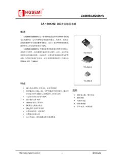
Transcription of 3A Step-Down Voltage Regulator
1 Available in TO-220 and TO-263,TO-220B packages(57V for HV version)The LM2596 / lm2596hv series operates at a switchingfrequency of150 kHz thus allowing smaller sized filter com-pontents than what would be needed with lower frequencyswitching regulators. Available in a standard 5-lead TO-220package with several different lead bend options, and a5-lesd TO-262 surface mount LM2596 / lm2596hv series of regulators are monolithicintegrated circuits that provide all the active functions for astep-down (buck) switching Regulator , capable of driving a 3 Aload with excellent line and load regulation.
2 These devicesare available in fixed output voltages of , 5V, 12V, and anadjustable output Step-Down Voltage RegulatorGeneral DescriptionRequiring a minimum number of external components, theseregulators are simple to use and include internal frequencycompensation , and a fixed-frequency standard series of inductors are available from severaldifferent manufacturers optimized for use with the LM2596series. This feature greatly simplifies the design ofswitch-mode power features include a guaranteed 4% tolerance on out-put Voltage under specified input Voltage and output loadconditions, and 15% on the oscillator frequency.
3 Externalshutdown is included, featuring typically 80 A standby cur-rent. Self protection features include a two stage frequencyreducing current limit for the output switch and an overtemperature shutdown for complete protection under , 5V, 12V, and adjustable output versionsnAdjustable version output Voltage range, to 37V 4% max over line and load conditionsnnGuaranteed 3A output load currentnInput Voltage range up to 40 VnRequires only 4 external componentsnExcellent line and load regulation specificationsn150 kHz fixed frequency internal oscillatornTTL shutdown capabilitynLow power standby mode, IQtypically 80 AnHigh efficiencynUses readily available standard inductorsnThermal shutdown and current limit protectionApplicationsnSimple high-efficiency Step-Down (buck)
4 RegulatornOn-card switching regulatorsnPositive to negative converterNote: Patent Number 5,382, Application(Fixed Output VoltageVersions)UMW LM2596/LM2596 HVUMW RUMW LM2596/LM2596 HVUMW LM2596/LM2596 HVLM2596 Package TypesTO220B-5L TO263-5L TO220-5 LSupply VoltageMaximum Supply VoltageAbsolute Maximum RatingsON /OFF Pin Input Voltage V +25 VFeedback Pin Voltage V +25 VOutput Voltage to Ground(Steady State) 1 VPower DissipationInternally limitedStorageTemperatureRange 65 Cto+150 CESD SusceptibilityHumanBodyModel 2kVLead TemperatureS PackageVapor Phase (60 sec.)
5 +215 CInfrared (10 sec.)+245 CT Package (Soldering, 10 sec.)+260 CMaximum Junction Temperature+150 COperating ConditionsTemperature Range 40 C TJ +125 C3A Step-Down Voltage RegulatorUMW LM2596/LM2596 HVUMW RUMW LM2596/LM2596 HVUMW LM2596/LM2596 HVPin AssignmentsPin Descriptions Name Description Vin Input supply Voltage Output Switching output Gnd Ground Feedback Output Voltage feedback ON/OFF ON/OFF shutdown Active is Low
6 Or floating 5 ON/OFF 4 Feedback 3 Gnd 2 Output 1 Vin 5 ON/OFF 4 Feedback3 Gnd 2 Output 1 Vin TO220B-5L/TO220-5L TO263-5L LM2596 TLM2596 SLM2596 HVTLM2596 HVTLM2596 SLM2596 SLM2596 HVTLM2596 HVTLM2596 SLM2596 HVSLM2596 HVSLM2596 HVSLM2596 HVSO rdering informationTemperatureRangeOutputVoltage ,VPackageType-40 C TA 125 , , ,LM2596 HVElectrical CharacteristicsSpecifications with standard type face are for TJ= 25 C, and those withboldface typeapply overfull Operating Tempera-ture RangeSymbolParameterConditionsUnits(Limi ts)TypLimitSYSTEM PARAMETERS(Note 5) Test CircuitFigure 1 VOUTO utput VIN 40V, ILOAD (min) (max) EfficiencyVIN= 12V, ILOAD=3A73%Electrical CharacteristicsSpecifications with standard type face are for TJ= 25 C, and those withboldface typeapply overfull Operating Tempera-ture RangeSymbolParameterConditionsUnits(Limi ts)TypLimitSYSTEM PARAMETERS(Note 5)
7 Test CircuitFigure 1 VOUTO utput Voltage7V VIN 40V, ILOAD (min) (max) EfficiencyVIN= 12V, ILOAD=3A80%Electrical CharacteristicsSpecifications with standard type face are for TJ= 25 C, and those withboldface typeapply overfull Operating Tempera-ture RangeSymbolParameterConditionsUnits(Limi ts)TypLimitSYSTEM PARAMETERS(Note 5) Test CircuitFigure 1 VOUTO utput Voltage15V VIN 40V, ILOAD (min) (max) EfficiencyVIN= 25V, ILOAD=3A90%3A Step-Down Voltage RegulatorUMW LM2596/LM2596 HVUMW RUMW LM2596/LM2596 HVUMW LM2596 lm2596hv -XXLM2596-ADJ, lm2596hv -ADJS pecifications with standard type face are for TJ= 25 C, and those withboldface typeapply overfull Operating Tempera-ture RangeSymbolParameterConditionsUnits(Limi ts)TypLimitSYSTEM PARAMETERS(Note 5) Test CircuitFigure 1 VFBF eedback VIN 40V, ILOAD for 3V.
8 Circuit ofFigure (min) (max) EfficiencyVIN= 12V, VOUT= 3V, ILOAD=3A73%All Output Voltage VersionsElectrical CharacteristicsSpecifications with standard type face are for TJ= 25 C, and those withboldface typeapply overfull Operating Tempera-ture Range. Unless otherwise specified, VIN= 12V for the , 5V, and Adjustable version and VIN= 24V for the 12V ver-sion. ILOAD= 500 mASymbolParameterConditionsLM2596-XXUnit s(Limits)TypLimitDEVICE PARAMETERSIbFeedback Bias CurrentAdjustable Version Only, VFB= (max)fOOscillator Frequency(Note 6)150kHz127/110kHz(min)173/173kHz(max)VS ATS aturation VoltageIOUT= 3A (Notes 7, 8) (max)DCMax Duty Cycle (ON)(Note 8)100%Min Duty Cycle (OFF)(Note 9)0 ICLC urrent LimitPeak Current (Notes 7, 8) (min) (max)ILOutput Leakage CurrentOutput = 0V (Notes 7, 9)50 A(max)Output = 1V (Note 10)2mA30mA(max)IQQuiescent Current(Note 9)5mA10mA(max)
9 ISTBYS tandby Quiescent Current ON/OFF pin = 5V (OFF)(Note 10)80 A200/250 A(max) JCThermal ResistanceTO-220 or TO-263 Package, Junction to Case2 C/W JATO-220 Package, Junction to Ambient (Note 11)50 C/W JATO-263 Package, Junction to Ambient (Note 12)50 C/W JATO-263 Package, Junction to Ambient (Note 13)30 C/W JATO-263 Package, Junction to Ambient (Note 14)20 C/WON/OFF CONTROLTest CircuitFigure 1ON /OFF Pin Logic VoltageLow ( Regulator ON) (max)VILHigh ( Regulator OFF) (min)3A Step-Down Voltage RegulatorUMW LM2596/LM2596 HVUMW RUMW LM2596/LM2596 HVUMW LM2596/LM2596 HVElectrical All Output Voltage VersionsElectrical Characteristics(Continued)Specifications with standard type face are for TJ= 25 C, and those withboldface typeapply overfull Operating Tempera-ture Range.
10 Unless otherwise specified, VIN= 12V for the , 5V, and Adjustable version and VIN= 24V for the 12V ver-sion. ILOAD= 500 mASymbolParameterConditionsUnits(Limits) TypLimitIHON /OFF Pin Input CurrentVLOGIC= ( Regulator OFF)5 A15 A(max)ILVLOGIC= ( Regulator ON) A5 A(max)Note 1:Absolute Maximum Ratings indicate limits beyond which damage to the device may occur. Operating Ratings indicate conditions for which the device isintended to be functional, but do not guarantee specific performance limits. For guaranteed specifications and test conditions, see the 2:The human body model is a 100 pF capacitor discharged through a resistor into each 3:Typical numbers are at 25 C and represent the most likely 4:All limits guaranteed at room temperature (standard type face) and at temperature extremes (bold type face).