Transcription of A Broadband HF Amplifier Using Low-Cost
1 40 March 1999 MBy Mike Kossor, WA2 EBY1 Notes appear on page ) from 160 through 10 meters. To thebasic Amplifier , I added an RF-sensed TRrelay and a set of low-pass filters designed tosuppress harmonic output and comply withFCC requirements. The Amplifier is built ondouble-sided PC board and requires no tun-ing. Another PC board contains the low-passfilters. Power-supply requirements are 28 Vdc at 5 A, although the Amplifier performswell at V of these amplifiers have been builtand exhibit similar performance. Al has beenusing his Amplifier on each of the HF bands,logging well over 500 contacts in 18 reports indicate a noticeable improve-ment in readability (about two S units on av-erage) over his 5 W rig. No indications of in-stability, CW key clicks or distortion on SSBhave been reported. To make it easy for you toduplicate this project, PC boards and parts kitsare available, all at a cost of about $100!
2 9An Overview of MOSFETsMOSFETs operate very differentlyfrom bipolar transistors. MOSFETs arevoltage-controlled devices and exhibit a veryhigh input impedance at dc, whereas bipolartransistors are current-controlled devices andhave a relatively low input impedance. Bias-ing a MOSFET for linear operation only re-quires applying a fixed voltage to its gate viaa resistor. With MOSFETs, no special bias orfeedback circuitry is required to maintain thebias point over temperature as is requiredwith bipolar transistors to prevent With MOSFETs, the gate-thresh-old voltage increases with increased draincurrent. This works to turn off the device,especially at elevated temperatures astransconductance decreases and RDS(on)(static drain-to-source on resistance) in-creases. These built-in self-regulating ac-tions prevent MOSFETs from being affectedFigure 1 Jim Wyckoff, AA3X, 1 W In, 30 W Out With Power MOSFETs at 80 M, Hintsand Kinks, QST, Jan 1993, pp articles have been writtenencouraging experimenters to usepower MOSFETs to build HF RFamplifiers.
3 That s because powerMOSFETs popular in the design of switch-ing power supplies cost as little as $1 each,whereas RF MOSFET prices start at about$35 each!Over the years, I tucked away several ofthese articles, waiting for an opportunity toexperiment with them. That opportunity camewhen I received a call from Al, W2 OBJ. Alwanted a Low-Cost linear Amplifier to use withhis 5 W QRP transmitter when band condi-tions got poor. Ideally, the Amplifier wouldgenerate at least 25 W on all the HF s inquiry renewed my interest in the topicand provided the motivation I needed to getmy project provided me with an extensive list ofRF- Amplifier construction articles that usepower These articles provideduseful information about MOSFETs and gen-eral guidelines for working with them, in-cluding biasing, parasitic-oscillation sup-pression, Broadband impedance-matchingtechniques and typical Amplifier performancedata.
4 It was clear from the performance datathat Al s desire to get 25 W output frompower MOSFETs on to 30 MHz was go-ing to be a challenge! The RF output power ofmost of the amplifiers described in the ar-ticles drops off to 10 W or less as frequencyincreases just to 14 Idea BrewsAfter hundreds of hours of experimenta-tion, I came up with a design that exceeds ouroriginal objective: One watt of input powerproduces over 40 W of output (after harmonicPar t 1 With only 1 W ofdrive, you ll get over40 W out from 160through 10 meters!A BroadbandHF AmplifierUsing Low-CostPower MOSFETsMarch 199941C1-C8 F chip (140-CC502Z104M)C9 47 pF chip (140-CC502N470J)C10 100 F, 35 V (140-HTRL35V100)C11, C13 15 F, 35 V (140 MLR35V10)C12 1 F, 50 V ( )C14 F, 35 V tantalum( )C15 F chip (140-CC502B103K)C16, C17 F chip(140-CC502B102K)D1 1N4733A, V, 1 W Zener diode(583-1N4733A)D4 1N4004A(583-1N4004A)D2, D3 1N4148 (583-1N4148)D5 1N4744A, 15 V, 1 W Zener diode(583-1N4744A)J1, J2 SO-239 UHF connector(523-81-120)Figure 2 Schematic of the MOSFET all-band HF Amplifier .)
5 Unless otherwise specified, resistors are 1/4 W, 5% tolerancecarbon-composition or film units. Equivalent parts can be substituted. Part numbers in parentheses are Mouser (Mouser Electronics,968 N Main St, Mansfield, TX 76063; tel 800-346-6873, 817-483-4422, fax 817-483-0931; sales@ ; ); see Note 12 V DPDT, 960 coil, mA(431-OVR-SH-212L)L1, L2 91/2 turns #24 enameled wire,closely wound IDL3 31/2 turns #24 enameled wire, closelywound IDQ1, Q2 IRF510 power MOSFET(570-IRF510)Q3 2N3904 (610-2N3904)R1, R2 10 k trim pot (323-5000-10K)R3, R4 27 , 1/2 W (293-27)R6 1 k chip (263-1K)R7 k chip ( )R8 130 , 1 W (281-130); for 7 dB pad(5 W in, 1 W out)R9 43 , 2 W (282-43); for 7 dB pad(5 W in, 1 W out)R10 130 , 3 W (283-130); for 7 dB pad(5 W in, 1 W out)R8, R10 300 , 1/2 W (273-300); for3 dB pad (2 W in, 1 W out)R9 18 , 1 W (281-18); for 3 dB pad(2 W in, 1 W out)R11 k , 1/2 W ( )T1 10 bifilar turns #24 enameled wire onan FT-50-43 10 bifilar turns #22 enameled wire ontwo stacked FT-50-43 Pri 2 turns, sec 3 turns #20 Teflon-covered wire on BN-43-3312 balun : Aluminum enclosure 8 6 inches(HWD) (537-TF-783), two TO-220mounting kits (534-4724), heat-sinkcompound (577-1977), Amplifier PC board(see Note 9), heat sink (AAVID [Mouser532-244609B02]; see text), about two feetof RG-58 coax, #24 enameled wire and#20 Teflon-insulated 1999by thermal runaway.
6 MOSFETs do not re-quire negative feedback to suppress low-fre-quency gain as is often required with bipolarRF transistors. Bipolar transistor gain in-creases as frequency decreases. Very highgain at dc and low frequencies can causeunwanted, low-frequency oscillation to oc-cur in bipolar transistor RF amplifiers unlessnegative feedback is employed to prevent oscillation can damage bipo-lar transistors by causing excess power dissi-pation, leading to thermal LimitationsOf course, MOSFETs do have their limi-tations. The high gate impedance and thedevice structure make them susceptible toelectrostatic discharge (ESD) damage. Someeasily applied precautions prevent this: Usea soldering iron with grounded tip; use a wriststrap connected to ground through a 1 M resistor to bleed off excess body chargewhile handling MOSFETs and do all work onan anti-static mat connected to ground via a1 M sensitivity of a MOSFET s gate tostatic and high-voltage spikes also makes itvulnerable to damage resulting from parasiticoscillation.
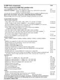
7 This undesired self-oscillationcould result in excessive gate-to-source volt-age that permanently damages the MOSFET sgate insulation. Another MOSFET limitationis gate capacitance. This parameter limits thefrequency at which a MOSFET can operateeffectively as an RF Amplifier . I recommendreviewing the referents of Notes 1, 2 and 3 ifyou are interested in more detailed informa-tion about MOSFET RF AmplifiersOf the several power MOSFET amplifiersI built to check their performance, the oneproviding the best performance is the push-pull design described by Jim Wyckoff, AA3X,in QST (see Note 3). I used IRF510 powerMOSFETs rather than the IRF511s performance of this power MOSFET Amplifier design is summarized in Figure 1;its basic design is very similar to anotheramplifier described in the referent of Note 4,written 10 years earlier. That Amplifier uses apair of more-expensive MRF138 MOSFET sdesigned specifically for RF Figure 1 shows, the Hints and Kinksamplifier performance is excellent from to 7 MHz and far exceeds the publishedfigure of 30 W output on MHz.
8 As fre-quency increases above 10 MHz, however,output drops off rapidly, falling below 10 Wabove 21 MHz. (These levels were measuredafter harmonic filtering.)Although the Amplifier is identified asstable, my first attempt at duplicating theamplifier resulted in oscillations that de-stroyed one of the IRF510s. I was puzzledby this. At first, I thought the problem wascaused by my substitution of the slightlymore robust IRF510 MOSFETs for thecalled-for IRF511s. That idea proved wrongwhen my second attempt to power up theamplifier with IRF511 MOSFETs installedalso resulted in a blown IRF511. (Thankgoodness these are $1 power MOSFETs, not$35 RF MOSFETs!) I finally achieved goodstability when I added a small amount ofinductance in series with the MOSFET source to ground (just two turns of #24 wire, inch diameter). With this added in-ductance, I was able to remove the ferritebeads from the circuit without any sign ofinstability.
9 I believe the substitution of theIRF510 and minimizing source lead induc-tance are the reasons I obtained significantlyhigher RF output power and wider band-width than described in the referent of Note3. This experiment underscores the need toobserve exact construction techniques andphysical layout if similar performance is tobe expected. Even though I used PC boardconstruction, I got significantly differentresults because my layout was not the sameas the author the DesignAlthough the Amplifier performed betterthan expected, its bandwidth was signifi-cantly less than desired. Considerable experi-mentation (and I do mean considerable!) re-sulted in the circuit shown in Figure 2. Thisamplifier consists of two power MOSFET soperating in push-pull and employs an RF-sensed TR receive, TR relay K1 is deener-gized. Signals from the antenna are connectedto J2 and routed through K1 to a transceiverconnected to J1.
10 (This path loss is less dB from MHz through 30 MHz.) Intransmit, RF voltage from the transceiver issampled by C17 and divided by R6 and and D3 rectify the RF voltage and chargeC16. Q3 begins conducting when the detectedRF voltage across C16 reaches V. This energizes K1, which then routesthe transmitted RF signal from J1 to the inputof the Amplifier and sends the output of theamplifier to the antenna at J2. RF-sensed re-lay response is very fast. No noticeable clip-ping of the first CW character has been made provisions to include an RF attenu-ator (consisting of R8, R9 and R10) to enableadjusting the Amplifier iput power to 1 W.(The parts list contains resistor values to re-duce the output of 2 or 5 W drivers to 1 W.)The 1 W signal is then applied to the primaryof T1 via an input impedance-matching net-work consisting of L3. T1 is a 1:1 balun thatsplits the RF signal into two outputs 180 de-grees out of phase.