Transcription of A25L016 - AMIC TECHNOLOGY
1 A25L016 Series 16 Mbit Low Voltage, Serial Flash Memory With 100 MHz Uniform 4KB Sectors (March, 2012, Version ) AMIC TECHNOLOGY Corp. Document Title 16 Mbit, Low Voltage, Serial Flash Memory With 100 MHz Uniform 4KB Sectors Revision History Rev. No. History Issue Date Remark Initial issue April 2, 2008 Final Add the spec.
2 Of ICC3 for 100 MHz December 26, 2008 Modify the ICC1 and ICC2 to 25 A Modify the ICC7 to 25mA Modify the tPP to 3ms Modify the tSE to Modify the Sector Erase Time to (typical) April 9, 2009 Modify the Page Program Time to 2ms (typical) Modify the Active Read Current to 35mA (Max.) Modify the Program/Erase Current to 25mA (Max.) Modify the Standby Current to 25 A (Max.) Modify Block Erase Cycle Time to (Max.) Modify Chip Erase Cycle Time to 40s (Max.) Add packing description in Part Numbering Scheme April 23, 2010 P30: Change Data Retention and Endurance value from 27, 2010 to Min.
3 Add 8-pin WSON (6*5mm) package type December 21, 2010 Change tW, tSE, tBE and tCE values August 19, 2011 P1: Add Provide 64 Bytes Security ID (application note is availableSeptember 20, 2011 by request) in Features Add 8-pin SOP (150mil) package type October 11, 2011 Change tSE(typ.) from to November 15, 2011 Change tSE(max.) from to Change tBE(typ,) from to P31: Change ICC6(max.) from 15mA to 25mA March 29, 2012 A25L016 Series 16 Mbit Low Voltage, Serial Flash Memory With 100 MHz Uniform 4KB Sectors (March, 2012, Version ) 1 AMIC TECHNOLOGY Corp.
4 FEATURES Family of Serial Flash Memories - A25L016 : 16M-bit /2M-byte Flexible Sector Architecture with 4KB sectors - Sector Erase (4K-bytes) in 80ms (typical) - Block Erase (64K-bytes) in 500ms (typical) Page Program (up to 256 Bytes) in 2ms (typical) to Single Supply Voltage Dual input / output instructions resulting in an equivalent clock frequency of 200 MHz: - Dual Output Fast Read Instruction - Dual Input and Output Fast Read Instruction SPI Bus Compatible Serial Interface 100 MHz Clock Rate (maximum) 16 Mbit Flash memory - Uniform 4-Kbyte sectors - Uniform 64-Kbyte blocks Electronic Signatures - JEDEC Standard Two-Byte Signature A25L016 .
5 (3015h) - RES Instruction, One-Byte, Signature, for backward compatibility A25L016 (14h) Package options - 8-pin SOP (150/209mil), 16-pin SOP (300mil), 8-pin DIP (300mil) or 8-pin WSON (6*5mm) - All Pb-free (Lead-free) products are RoHS compliant Provide 64 Bytes Security ID (application note is available by request) GENERAL DESCRIPTION The A25L016 is 16M bit Serial Flash Memory, with advanced write protection mechanisms, accessed by a high speed SPI-compatible bus. The memory can be programmed 1 to 256 bytes at a time, using the Page Program instruction.
6 The memory is organized as 32 blocks, each containing 16 sectors. Each sector is composed of 16 pages. Each page is 256 bytes wide. Thus, the whole memory can be viewed as consisting of 8,192 pages, or 2,097,152 bytes. The whole memory can be erased using the Chip Erase instruction, a block at a time, using Block Erase instruction, or a sector at a time, using the Sector Erase instruction. Pin Configurations SOP8 Connections SOP16 Connections VCCCDODIOSWHOLDVSS1 82 73 64 5A25L016 VCCCDUDOSHOLDVSS1 162 153 144 135 126 117 108 9A25L016 DUDUDUDIODUDUDUDUWNote:DU = Do not Use A25L016 Series (March, 2012, Version ) 2 AMIC TECHNOLOGY Corp.
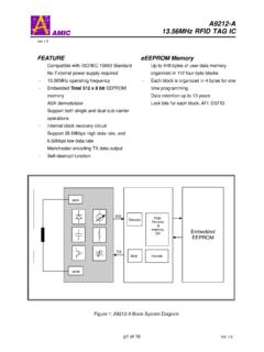
7 Pin Configurations (Continued) DIP8 Connections WSON8 Connections A25L016 VCCCDODIOSWHOLDVSS1 82 73 64 5 VCCCDODIOSWHOLDVSSA25L01612348765 Block Diagram Control LogicHigh VoltageGeneratorI/O Shift RegisterAddress registerand Counter256 ByteData BufferStatusRegisterX Decoder256 Byte (Page Size)Y DecoderSize of thememory areaDIODOC000 FFh00000hHOLDWS1 FFFFF A25L016 Series (March, 2012, Version ) 3 AMIC TECHNOLOGY Corp. Pin Descriptions Pin No. Description C Serial Clock DIO Serial Data Input 1 DO Serial Data Output 2 S Chip Select W Write Protect HOLD Hold VCC Supply Voltage VSS Ground Notes: 1.
8 The DIO is also used as an output pin when the Fast Read Dual Output instruction and the Fast Read Dual Input-Output instruction are executed. 2. The DO is also used as an input pin when the Fast Read Dual Input-Output instruction. Logic Symbol A25L016 DODIOSWHOLDVSSVCCC SIGNAL DESCRIPTION Serial Data Output (DO). This output signal is used to transfer data serially out of the device. Data is shifted out on the falling edge of Serial Clock (C). The DO pin is also used as an input pin when the Fast Read Dual Input-Output instruction and Dual Input Fast Program is executed.
9 Serial Data Input (DIO). This input signal is used to transfer data serially into the device. It receives instructions, addresses, and the data to be programmed. Values are latched on the rising edge of Serial Clock (C). The DIO pin is also used as an output pin when the Fast Read Dual Output instruction and the Fast Read Dual Input-Output instruction are executed. Serial Clock (C). This input signal provides the timing of the serial interface. Instructions, addresses, or data present at Serial Data Input (DIO) are latched on the rising edge of Serial Clock (C).
10 Data on Serial Data Output (DO) changes after the falling edge of Serial Clock (C). Chip Select (S). When this input signal is High, the device is deselected and Serial Data Output (DO) is at high impedance. Unless an internal Program, Erase or Write Status Register cycle is in progress, the device will be in the Standby mode (this is not the Deep Power-down mode). Driving Chip Select (S) Low enables the device, placing it in the active power mode. After Power-up, a falling edge on Chip Select (S) is required prior to the start of any instruction.