Transcription of ASSOCIATION CONNECTING ELECTRONICS …
1 IPC/JEDEC-9704 printed Wiring BoardStrain Gage Test GuidelineDeveloped by the JEDEC Reliability Test Methods for Packaged DevicesCommittee ( ) and the SMT Attachment Reliability Test MethodsTask Group (6-10d) of the Product Reliability Committee (6-10) of IPCU sers of this publication are encouraged to participate in thedevelopment of future :IPC3000 Lakeside Drive, Suite 309 SBannockburn, Illinois60015-1219 Tel 847 847 CONNECTINGELECTRONICS INDUSTRIES Table of .. and Definitions .. 22 APPLICABLE .. Publications .. 23 GENERAL .. and Gage .. Attachment .. Calibration .. Simulation .. Package Test .. 114 DATA ANALYSIS AND Frequency .. Gage Test Report 12 APPENDIX ASTRAIN 14 APPENDIX BREFERENCE FOR RATE 16 APPENDIX CICT DESIGN 18 APPENDIX 19 FiguresFigure 1-1 Lifted 1 Figure 3-1 board Assembly Strain Measurement.
2 3 Figure 3-2 System Assembly Strain 3 Figure 3-3 board with SMT Components Only(After SMT Reflow) Example 4 Figure 3-4 board with SMT Components Only(After SMT Reflow) Example 4 Figure 3-5 board with Both SMT and Through-HoleComponents (After Wave Solder).. 4 Figure 3-6 ICT Fixture Strain Gage Test Setup .. 5 Figure 3-7 Stacked Rosette Strain Gage .. 5 Figure 3-8 Strain Gage Dimensions (Inches) .. 6 Figure 3-9 Recommended Gage Placement .. 7 Figure 3-10 Interference Due to BGA Pushdown Block .. 8 Figure 3-11 Interference Due to ICT Probe .. 8 Figure 3-12 Centroid of Gage Placement AboveCorner Land Pad .. 9 Figure 3-13 Component Removal to Facilitate GagePlacement .. 9 Figure 3-14 Lead Wire Routing Example 1 .. 10 Figure 3-15 Lead Wire Routing Example 2 .. 10 Figure 3-16 Gage Correlation Tool .. 11 Figure 3-17 Simulated Edge Guides .. 11 Figure 3-18 Shipping Package Drop Test.
3 12 Figure 3-19 Placement of Instrumented Boards forShipping Package Test .. 12 Figure 4-1 Time History of the Strain Limit Criteria .. 12 Figure A-1 Typical Example of Allowable Strainas a Function of Strain Rate and BoardThickness .. 15 Figure B-1 Data Reporting Example for mmThick PWB .. 17 IPC/JEDEC-9704 June 2005ivPrinted Wiring BoardStrain Gage Test Guideline1 SCOPEThis document describes specific guidelines for strain gagetesting for printed Wiring board (PWB) assemblies in theboard manufacturing process including, assembly, test, sys-tem integration and board suggested procedure enables board assemblers to con-duct required strain gage testing independently, and pro-vides a quantitative method for measuring board flexure,and assessing risk topics covered include: Test setup and equipment requirements Strain measurement Report formatThis document assumes a surface mount device; Ball GridArray (BGA), Small Outline Package (SOP) and ChipScale (Size) Package (CSP) are typical device Surface Mount Technology (SMT) devices, ( ,capacitors, resistors, etc.)
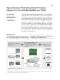
4 Are outside the scope of this PurposeStrain gage testing allows objective analy-sis of the strain and strain rate levels that a SMT packageis subjected to during PWB assembly, test and of worst-case PWB strain is critical due tothe susceptibility of component solder joints to strain-induced failures. Excessive strain can result in solder jointdamage for all package substrate plating finishes. Such fail-ures include solder ball cracking, trace damage, pad lifting(shown in Figure 1-1) and substrate cracking during boardmanufacturing and test BackgroundBoard flexure control using strain gagemeasurement has proven very beneficial to the electronicsindustry, and continues to gain acceptance as a method toidentify damaging manufacturing processes. However, asinterconnect densities have increased and become morefragile, the potential for flexure-induced damage hasincreased.
5 Many board assemblers are now required tooperate under strain levels specified by their customers orcomponent strain measurement technology has matured, differentmethodologies have developed. Variations in strain gagemethodology inhibit reliable data collection and preventdata comparison across the industry. This documentaddresses variations in gage mounting, gage placement,experiment design, data acquisition system variables, andstrain strain measurement includes application of straingages to the board at specified components, and then sub-jecting the instrumented board to various test and assemblyoperations. Test and assembly steps which exceed strainlimits are deemed excessive and are identified so that cor-rective actions can be made. Strain limits may come fromthe customer, component supplier or internal best knownpractices.
6 Examples of strain measurement criteria areshown in Appendix identifying areas sensitive to manufacturing variation,strain gage testing provides insight into the effects of aproduction ramp. Strain gage measurements become thebaseline for future process improvement activities, andquantify the effectiveness of adjustments. Manufacturingsteps that are typically characterized are listed below:1. SMT assembly process: board depanelization (routing) processes All manual handling processes All rework and retouch processes Connector installation Component installation2. board test processes: In-Circuit Test (ICT) board Functional Test (BFT), or equivalent functionaltest3. Mechanical assembly: Heat sink assembly board support/stiffener assemblyFigure 1-1 Lifted PadBGA solder ballcopper padFR4 boardcrackJune 2005 IPC/JEDEC-97041