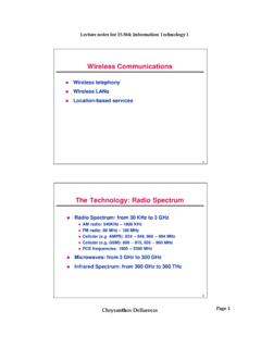
Transcription of Conductivity in semiconductors. Engineering conductivity ...
1 Lecture 17. Conductivity in semiconductors . Engineering Conductivity through doping. Today: 1. semiconductors under applied electric field. Origins of Conductivity . 2. Evanescent states inside the bandgap. 3. Impurities in semiconductors . 4. Engineering Conductivity through doping. 5. Carrier densities in p- and n-doped semiconductors . 6. Fermi level in doped semiconductors . Questions you should be able to answer by the end of today's lecture: 1. What carriers participate in conduction in semiconductors ? How does conduction in a semiconductor differ from a metal? 2. What is the physical significance of evanescent states inside the bandgap? 3. What are dopants? What dopants are used to make p-type and n-type semiconductors ? What are deep-trap dopants? 4. How does doping affect the density of carriers in SC? 5. How to find the concentration of the minority carriers in a doped SC? 6. How do we use doping to engineer chemical potential (Fermi level)?
2 7. How does carrier density change with temperature in extrinsic (doped) SC? 8. How does the Conductivity in SC change with temperature? How is it different from metals? 1. What happens when we apply voltage to a piece of semiconductor? How do carriers respond to applied electric field? From introductory physics we remember that electron motion is governed by the Lorentz force: 1 . F e E v B , . c . where E is electric field, B is magnetic field and v is electron velocity.. dv From Newtonian mechanics we remember: F m . dt . dv eE. Then in the absence of magnetic field, we find: m eE v t v 0 t dt m On average the velocity of the electrons inside the solid is zero in the absence of magnetic. eEt Consequently we find: v t . m Definition: current density. The current density is defined as number of charge carriers per area per unit time and is expressed as: N. j n q v , where n is the carrier density and q is carrier charge. V. Then for electrons moving under applied electric field we can write: ne2 t ne2 t j n e v E E , where is the electron Conductivity of the material.
3 M m From our simple calculation it looks like the Conductivity depends on time, which is obviously not true for most materials. Electrons moving through the material collide with the lattice other electrons, impurities etc. Consequently, the time of free flight will be limited for electrons inside the material. Generally, we can write the following dependence of the velocity on the applied field: eE . v t , where is the average time between collisions. m ne2 . Then the electron Conductivity is defined as: . m The calculation above is purely classical. So what happens when we look at quantum particles? Remember the group velocity, which is average velocity with which particles propagate through 1 E dv 1 d E 1 2 E dk 1 2 E dk 1 dk a periodic potential: vg g . k dt dt k k 2 dt 2 k 2 dt me* dt 2. Above we used the definition of the effective mass inside the periodic potential, which we have found to be inversely proportional to the curvature of the band.
4 While in periodic materials k is crystal momentum and not momentum, it is still possible to show dk that: F . dt Remembering that F eE and taking the equation above into account we find: dvg F eE eE. * * vg t * t . dt me me me Analogously to the classical case we do not use the time but rather the average time between eE . collisions inside the material, which leads us to: vg * e . me ne 2 e Which results in the electron Conductivity of the material: . me*. However, we forgot an important detail, in semiconductors the conduction may happen via electrons or holes, which means we have to add the hole Conductivity to obtain the total Conductivity of our semiconductor: nc e p . nc e *. pv e v *h mc mv nc e p . e *. , h v *h mc mv Where e and h is the mobility of the electrons and holes respectively. As we can see the mobilities are related to the band curvature through the effective mass parameter, such that larger effective masses will lead to smaller mobilities.
5 (This makes sense from the inertial prospective). Carrier mobilities at room temperature, in cm2/V-s Crystal Electrons Holes Crystal Electrons Holes Diamond 1800 1200 GaAs 8000 300. Si 1350 480 GaSb 5000 1000. Ge 3600 1800 PbS 550 600. InSb 800 450 PbSe 1020 930. InAs 30000 450 PbTe 2500 1000. InP 4500 100 AgCl 50 - AlAs 280 - KBr (100 K) 100 - AlSb 900 400 Sic 100 10-20. Image by MIT OpenCourseWare. Also note that Conductivity in SC increases with temperature since the nc and pv increase with temperature. This is exactly opposite from metals, where Conductivity decreases with temperature, since the n stays the same, while drops rapidly due to increased collisions. 3. The effect of impurities: Engineering Conductivity through doping. We analyzed the solutions near the band edge by retaining the first two terms in our series solution near k g 2 . Let us now examine another possibility, which we have neglected up until now. Let us now allow for k to be complex: k g 2 ik '.
6 This yields the following truncated matrix for the central equation for the simple potential V x 2V cos gx . 2. 2 2 2 . g 2 . V E . 2 g . ik E V 2m 2 . 2m 2 2 2 . 0 k . 2. 2m 2. 2 g .. 2. g V ik E 2m 2m 2 . g Above we use the approximation k . 2. Figure removed due to copyright restrictions. Fig. 12: Kittel, Charles. Introduction to Solid State Physics. 8th ed. Wiley, 2004, p. 196. This means that there are evanescent (decaying) solutions that penetrate into the band gap. Through these decaying states the electrons can move from or into the defect states produced by the impurities. Impurities that have their electronic energy levels close to the conduction band end up donating their electrons into the conduction band and are called donors . These impurities contribute to electronic Conductivity in semiconductor and result in n-doping . Impurities that have their electronic energy levels close to the valence band extract electrons from the valence band leaving behind holes and are called acceptors.
7 These impurities contribute to hole Conductivity in semiconductor and result in p-doping . Impurities with their electronic energy level close to the middle of the energy gap end up trapping electrons that would have otherwise moved from valence to conduction band and hence reduce the number of conduction electrons and decrease the overall Conductivity . These impurities are called deep traps and are generally avoided by semiconductor manufacturers. 4. Impurity levels with respect to bands in Si, Ge and GaAs (typical semiconductors ). Figure removed due to copyright restrictions. Fig. : Unknown source. 5. Semiconductor carrier Engineering : Extrinsic semiconductors Adding very small amounts of impurities can drastically change the Conductivity of the semiconductor and define the conduction type, make it largely electron-conductive (n-type). or hole conductive (p-type). semiconductors doped with donor or acceptor atoms to engineer their Conductivity are called extrinsic.
8 Adding impurities to determine carrier type: Intrinsic carrier concentration in Si at room temperature: Eg . 2. n N e Pv e ~ 1020 cm 6 ni ~ 1010 cm 3. k BT. i While the total density of atoms in Si is ~1022 cm-3. If we add just 1016 cm-3 (~1ppm) of Phosphorous atoms, which act as donors for Si, the concentration of electrons in the conduction band will be approximately to that of Phosphorous atoms: nc N D 1016 cm 3 . This is 6 orders of magnitude more electrons then in the intrinsic Si! N-doped Si in this case will be a million times more conductive then the pure Si! In addition using the Law of Mass Action we can find the concentration of holes: ni2 10 20. nc pv ni2 10 20 pv 16 10 4 cm 3. nc 10. As you can see the concentration of holes will be 6 orders of magnitude lower than the concentration of electrons, which simply means that your Conductivity will mostly come from electrons. Analogously if you dope Si with Boron, which acts as an acceptor resulting in p-type Si, you can find that the concentration of electrons will be orders of magnitude lower than that of holes and consequently the Conductivity will be dominated by holes.
9 For n-type material at room temperature: For p-type material at room temperature: nc N D pv N A. ni2 ni2. pv nc . ND NA. 6. Temperature behavior of doped semiconductors Figure removed due to copyright restrictions. Fig. : Pierret, Robert F. Semiconductor Fundamentals. 2nd e d. Prentice Hall, 1988. At T=0 K electrons of the semiconductor occupy only the states below Fermi level, the valence band, and the electrons of the dopant (in the picture donor) are staying within the donor level. There is no conduction. nc 0. At low T some electrons get promoted from the donor level into the conduction band contributing to the conduction. Very few electrons will be promoted from the valence into the conduction band, so the Conductivity will be completely determined by the electrons donated by the ionized donors. nc N D . At moderate T all donors will be ionized from contributing their electrons to the conduction band and a small number electrons from the valence band would be promoted to the conduction band.
10 Nc N D. At high T a lot of electrons from the valence band would get promoted to the conduction band completely swamping the electrons from the donor. The doped semiconductor in this case would behave like an intrinsic semiconductor. nc ni 7. Calculating the Fermi level in doped semiconductors . We can find the position of the chemical potential or the Fermi level from the condition of the charge neutrality, material cannot be charged or it becomes unstable. This means that for generally doped semiconductors that contains both donor and acceptor impurities we need to balance the number of electrons in the conductions band nc , the number of holes in the valence band pv , and the numbers of ionized donors and acceptors N D and N A . pv nc N D N A 0. Substituting the relevant equations from the previous lecture: ND NA. Pv e . Ev EF kBT. N c e . EF Ec kBT. EF E D . EA EF . 0. 1 2e 1 2e kB T kB T. Using the equation above we can find the EF. Generally we find that the Fermi level of the n-doped semiconductor is above the Fermi level of the intrinsic semiconductor, while the Fermi level of the p-doped semiconductor is below the intrinsic Fermi level.