Transcription of Cool-Power ZVS Switching Regulators
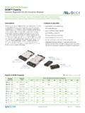
1 Cool-Power ZVS Switching Regulators Rev 1 of 49 08/20178V 60 VIN , 10V 50 VOUT , 50 140W Cool-Power ZVS Buck-Boost RegulatorCool-Power ZVS Switching RegulatorsPI3740-00 Product DescriptionThe PI3740-00 is a high efficiency, wide input and output range DC-DC ZVS Buck-Boost Regulator. This high density System-in-Package (SiP) integrates controller, power switches, and support components. The integration of a high performance Zero-Voltage Switching (ZVS) topology within the PI3740-00 increases point of load performance, providing best in class power PI3740-00 requires an external inductor, resistive divider and minimal capacitors to form a complete DC DC Switching mode buck-boost ZVS architecture also enables high frequency operation while minimizing Switching losses and maximizing efficiency.
2 The high Switching frequency operation reduces the size of the external filtering components, improves power density, and enables fast dynamic response to line and load & Benefits Up to 96% efficiency 50 140W continuous output power Parallel capable with single wire current sharing External frequency synchronization / interleaving High Side Current Sense Amplifier General Purpose Amplifier Lighting / Constant Current Mode (LGH) Input Over / Undervoltage Lockout (OVLO / UVLO) Output Overvoltage Protection (OVP) Overtemperature Protection (OTP) Fast and slow current limits -40 C to 115 C operating range (TJ)
3 Excellent light load efficiencyApplications Battery Charging and Conditioning, Telecom, Networking, Lighting Computing, Communications, Industrial, Automotive Accessories 12V, 24V, 48V and 60V DC DC ApplicationsPackage Information 10mm x 14mm x LGA SiPPI3740-0010kCINVINPGNDVS1VS2 VOUTISPPGNDISNIMONVSNVSPCOMPEAOEAINVDIFF LGHCOUTR1R2 CHFCCOMPSYNC ITRKSGNDENSYNC OPGDVDRCTRKT ypical ApplicationDeviceOutput VoltageSetRangePI3740-00-LGIZ12V10 to 50 VCool-Power ZVS Switching Regulators Rev 2 of 49 08/2017PI3740-00 ContentsOrder Information 3 Absolute Maximum Ratings 3 Pin Description 4 Package Pin-Out 5 Large Pin Blocks 5 Storage and Handling Information 6 Block Diagram
4 6PI3740-00-LGIZ Electrical Characteristics 7PI3740-00-LGIZ Performance Characteristics 11 MTBF 19 Functional Description 20 Enable 20 Switching Frequency Synchronization 20 Soft-Start and Tracking 20 Remote Sensing Differential Amplifier 20 Power Good 20 Output Current Limit Protection 20 Input Undervoltage Lockout 20 Input Overvoltage Lockout 20 Output Overvoltage Protection 21 Overtemperature Protection 21 Pulse Skip Mode (PSM)
5 21 Variable Frequency Operation 21 IMON Amplifier 21 Application Description 22 Output Voltage Trim 22 Soft-Start Adjustment and Tracking 22 Inductor Pairing 22 Filter Considerations 23PI3740-00 Maximum COUT Capability at Startup 26 Thermal Design 27 Thermal Design Inductor 29PI3740-00-LGIZ Percentage of SiP Loss to Total Loss 31 Evaluation Board Thermal De-rating 33 Parallel Operation 35 Synchronization 35 Interleaving 35 Small Signal Models CV-CC Modes 36 Small Signal Model Constant Voltage Mode 36 Error Amplifier 36 Lighting Mode (LGH)
6 36 LGH Amplifier Small Signal Model 37 VDR Bias Regulator 37PI3740-00-LGIZ Modulator Gain / Output Resistance 38 System Design Considerations 45 Package Drawings 46 Receiving PCB Pattern Design Recommendations 47 Revision History 48 Product Warranty 49 Cool-Power ZVS Switching Regulators Rev 3 of 49 08/2017PI3740-00 Order InformationAbsolute Maximum RatingsNote: Stresses beyond these limits may cause permanent damage to the device. Operation at these conditions or conditions beyond those listed in the Electrical Specifications table is not guaranteed.
7 All voltage nodes are referenced to PGND unless otherwise noted.[1] Transient VS1 voltages are guaranteed by design when the specified 420nH 10% inductor is used.[2] Non-Operating Test Mode Limits.[3] The ISP pin to ISN pin has a maximum differential limit of + and NumberDescriptionPackageTransport MediaMFGPI3740-00-LGIZVIN 8 60V, VOUT 10 50V10mm x 14mm 108-pin LGATRAYV icorLocationNameVMAXVMINISOURCEISINK1 2, G [2]40A [2]4 5, G [1]40A [2]18A [2]10 11, G [1]40A [2]18A [2]13 14, G [2]40A [2] [3]75V-2 VDC5mA5mA14 EISP [3]75V-2 VDC5mA5mA10 14, B + 10 12, C 9, B E + 7 8, F KPGNDN/AN/A18A [2]18A [2]
8 Cool-Power ZVS Switching Regulators Rev 4 of 49 08/2017PI3740-00 Pin DescriptionPin NumberPin NameDescription1 2, G KVINI nput voltage and sense node for UVLO, OVLO and feed forward 5, G KVS1 Input side Switching node and ZVS sense node for power 11, G KVS2 Output side Switching node and ZVS sense node for power 14, G KVOUTO utput voltage and sense node for power switches, VOUT feed forward compensation, VOUT_OV and internal supply for gate drivers and internal logic. May be used as reference or low power bias supply for up to 2mA.
9 Must be impedance limited by the & Power Good indicator. PGD pulls low when the regulator is not operating or if EAIN is less than output. Outputs a high signal for of the programmed Switching period at the beginning of each Switching cycle, for synchronization of other Regulators . 1 BSYNCIS ynchronization input. When a falling edge synchronization pulse is detected, the PI3740-00 will delay the start of the next Switching cycle until the next falling edge sync pulse arrives, up to a maximum delay of two times the programmed Switching period.
10 If the next pulse does not arrive within two times the programmed Switching period, the controller will leave sync mode and start a Switching cycle automatically. Connect to SGND when not in use. 1 AFT1 For factory use only. Connect to SGND or leave floating in factory use only. Connect to SGND or leave floating in factory use only. Connect to SGND in factory use only. Connect to SGND in Enable control. Asserted high or left floating regulator enabled;Asserted low, regulator output disabled.