Transcription of DMOS Microstepping Driver with Translator And Overcurrent ...
1 A4988. DMOS Microstepping Driver with Translator And Overcurrent Protection Features and Benefits Description Low RDS(ON) outputs The A4988 is a complete Microstepping motor Driver with Automatic current decay mode detection/selection built-in Translator for easy operation. It is designed to operate Mixed and Slow current decay modes bipolar stepper motors in full-, half-, quarter-, eighth-, and Synchronous rectification for low power dissipation sixteenth-step modes, with an output drive capacity of up to Internal UVLO 35 V and 2 A. The A4988 includes a fixed off-time current Crossover-current protection regulator which has the ability to operate in Slow or Mixed and 5 V compatible logic supply decay modes. Thermal shutdown circuitry Short-to-ground protection The Translator is the key to the easy implementation of the Shorted load protection A4988.
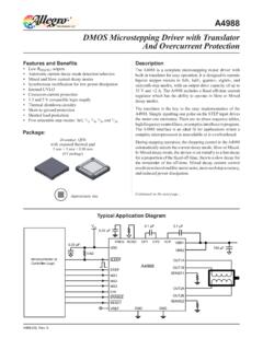
2 Simply inputting one pulse on the STEP input drives Five selectable step modes: full, 1/2, 1/4, 1/8, and 1/16 the motor one microstep. There are no phase sequence tables, high frequency control lines, or complex interfaces to program. The A4988 interface is an ideal fit for applications where a Package: complex microprocessor is unavailable or is overburdened. 28-contact QFN. with exposed thermal pad During stepping operation, the chopping control in the A4988. 5 mm 5 mm mm automatically selects the current decay mode, Slow or Mixed. (ET package) In Mixed decay mode, the device is set initially to a fast decay for a proportion of the fixed off-time, then to a slow decay for the remainder of the off-time. Mixed decay current control results in reduced audible motor noise, increased step accuracy, and reduced power dissipation. Continued on the next page.
3 Approximate size Typical Application Diagram VDD F F. F. VREG ROSC CP1 CP2 VCP VBB1. F. VDD 100 F. VBB2. 5 k . Microcontroller or SLEEP OUT1A. Controller Logic A4988 OUT1B. STEP. SENSE1. MS1. MS2. MS3. OUT2A. DIR. ENABLE OUT2B. RESET SENSE2. VREF GND GND. 4988-DS, Rev. 5. A4988 DMOS Microstepping Driver with Translator And Overcurrent Protection Description (continued). Internal synchronous rectification control circuitry is provided The A4988 is supplied in a surface mount QFN package (ES), 5 mm to improve power dissipation during PWM operation. Internal 5 mm, with a nominal overall package height of mm and an circuit protection includes: thermal shutdown with hysteresis, exposed pad for enhanced thermal dissipation. It is lead (Pb) free undervoltage lockout (UVLO), and crossover-current protection. (suffix T), with 100% matte tin plated leadframes.
4 Special power-on sequencing is not required. Selection Guide Part Number Package Packing A4988 SETTR-T 28-contact QFN with exposed thermal pad 1500 pieces per 7-in. reel Absolute Maximum Ratings Characteristic Symbol Notes Rating Units Load Supply Voltage VBB 35 V. Output Current IOUT 2 A. Logic Input Voltage VIN to V. Logic Supply Voltage VDD to V. Motor Outputs Voltage to 37 V. Sense Voltage VSENSE to V. Reference Voltage VREF V. Operating Ambient Temperature TA Range S 20 to 85 C. Maximum Junction TJ(max) 150 C. Storage Temperature Tstg 55 to 150 C. Allegro MicroSystems, LLC 2. 115 Northeast Cutoff Worcester, Massachusetts 01615-0036 ; A4988 DMOS Microstepping Driver with Translator And Overcurrent Protection Functional Block Diagram F F. VREG ROSC CP1 CP2. VDD Current Charge OSC. Regulator Pump VCP. F. DMOS Full Bridge VBB1. REF. DAC OUT1A.
5 OUT1B. PWM Latch Blanking OCP. Mixed Decay SENSE1. STEP. DIR Gate Drive DMOS Full Bridge RS1. VBB2. RESET. Control Translator MS1 Logic OUT2A. MS2 OCP. OUT2B. MS3. PWM Latch ENABLE Blanking SENSE2. Mixed Decay SLEEP. RS2. DAC. VREF. Allegro MicroSystems, LLC 3. 115 Northeast Cutoff Worcester, Massachusetts 01615-0036 ; A4988 DMOS Microstepping Driver with Translator And Overcurrent Protection ELECTRICAL CHARACTERISTICS1 at TA = 25 C, VBB = 35 V (unless otherwise noted). Characteristics Symbol Test Conditions Min. Max. Units Output Drivers Load Supply Voltage Range VBB Operating 8 35 V. Logic Supply Voltage Range VDD Operating V. Source Driver , IOUT = A 320 430 m . Output On Resistance RDSON. Sink Driver , IOUT = A 320 430 m . Source Diode, IF = A V. Body Diode Forward Voltage VF. Sink Diode, IF = A V. fPWM < 50 kHz 4 mA. Motor Supply Current IBB.
6 Operating, outputs disabled 2 mA. fPWM < 50 kHz 8 mA. Logic Supply Current IDD. Outputs off 5 mA. Control Logic VIN(1) VDD V. Logic Input Voltage VIN(0) VDD V. IIN(1) VIN = VDD 20 < 20 A. Logic Input Current IIN(0) VIN = VDD 20 < 20 A. RMS1 MS1 pin 100 k . Microstep Select RMS2 MS2 pin 50 k . RMS3 MS3 pin 100 k . Logic Input Hysteresis VHYS(IN) As a % of VDD 5 11 19 %. Blank Time tBLANK 1 s OSC = VDD or GND 20 30 40 s Fixed Off-Time tOFF. ROSC = 25 k 23 30 37 s Reference Input Voltage Range VREF 0 4 V. Reference Input Current IREF 3 0 3 A. VREF = 2 V, %ITripMAX = 15 %. Current Trip-Level Error3 errI VREF = 2 V, %ITripMAX = 5 %. VREF = 2 V, %ITripMAX = 5 %. Crossover Dead Time tDT 100 475 800 ns Protection Overcurrent Protection Threshold4 IOCPST A. Thermal Shutdown Temperature TTSD 165 C. Thermal Shutdown Hysteresis TTSDHYS 15 C. VDD Undervoltage Lockout VDDUVLO VDD rising V.
7 VDD Undervoltage Hysteresis VDDUVLOHYS 90 mV. 1 For input and output current specifications, negative current is defined as coming out of (sourcing) the specified device pin. 2 Typical data are for initial design estimations only, and assume optimum manufacturing and application conditions. Performance may vary for individual units, within the specified maximum and minimum limits. 3V. ERR = [(VREF/8) VSENSE] / (VREF/8). 4 Overcurrent protection (OCP) is tested at T = 25 C in a restricted range and guaranteed by characterization. A. Allegro MicroSystems, LLC 4. 115 Northeast Cutoff Worcester, Massachusetts 01615-0036 ; A4988 DMOS Microstepping Driver with Translator And Overcurrent Protection THERMAL CHARACTERISTICS. Characteristic Symbol Test Conditions* Value Units Package Thermal Resistance R JA Four-layer PCB, based on JEDEC standard 32 C/W.
8 *Additional thermal information available on Allegro Web site. Power Dissipation versus Ambient Temperature Power Dissipation, PD (W). R. J. A =. 32. C. /W. 0. 20 40 60 80 100 120 140 160. Temperature, TA ( C). Allegro MicroSystems, LLC 5. 115 Northeast Cutoff Worcester, Massachusetts 01615-0036 ; A4988 DMOS Microstepping Driver with Translator And Overcurrent Protection tA tB. STEP. tC tD. MS1, MS2, MS3, RESET, or DIR. Time Duration Symbol Typ. Unit STEP minimum, HIGH pulse width tA 1 s STEP minimum, LOW pulse width tB 1 s Setup time, input change to STEP tC 200 ns Hold time, input change to STEP tD 200 ns Figure 1: Logic Interface Timing Diagram Table 1: Microstepping Resolution Truth Table MS1 MS2 MS3 Microstep Resolution Excitation Mode L L L Full Step 2 Phase H L L Half Step 1-2 Phase L H L Quarter Step W1-2 Phase H H L Eighth Step 2W1-2 Phase H H H Sixteenth Step 4W1-2 Phase Allegro MicroSystems, LLC 6.
9 115 Northeast Cutoff Worcester, Massachusetts 01615-0036 ; A4988 DMOS Microstepping Driver with Translator And Overcurrent Protection Functional Description Device Operation. The A4988 is a complete Microstepping the home position which is by default common to all step modes. motor Driver with a built-in Translator for easy operation with minimal control lines. It is designed to operate bipolar stepper Mixed Decay Operation. The bridge operates in Mixed motors in full-, half-, quarter-, eighth, and sixteenth-step modes. decay mode, at power-on and reset, and during normal running The currents in each of the two output full-bridges and all of the according to the ROSC configuration and the step sequence, as N-channel DMOS FETs are regulated with fixed off-time PWM shown in Figures 9 through 13. During Mixed decay, when the (pulse width modulated) control circuitry.
10 At each step, the current trip point is reached, the A4988 initially goes into a fast decay for each full-bridge is set by the value of its external current-sense mode for of the off-time, tOFF . After that, it switches to resistor (RS1 and RS2), a reference voltage (VREF), and the output Slow decay mode for the remainder of tOFF. A timing diagram for voltage of its DAC (which in turn is controlled by the output of this feature appears on the next page. the Translator ). Typically, mixed decay is only necessary when the current in the At power-on or reset, the Translator sets the DACs and the phase winding is going from a higher value to a lower value as determined current polarity to the initial Home state (shown in Figures 9 by the state of the Translator . For most loads automatically-selected through 13), and the current regulator to Mixed Decay Mode for mixed decay is convenient because it minimizes ripple when the both phases.