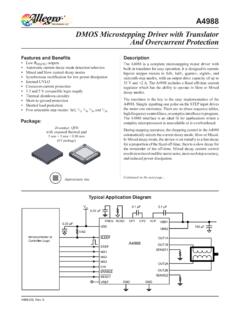
Transcription of DMOS Microstepping Driver with Translator And Overcurrent ...
1 Features and Benefits Low RDS(ON) outputs Automatic current decay mode detection/selection Mixed and Slow current decay modes Synchronous rectification for low power dissipation Internal UVLO Crossover-current protection and 5 V compatible logic supply Thermal shutdown circuitry Short-to-ground protection Shorted load protection Five selectable step modes: full, 1/2, 1/4, 1/8, and 1/16 Package:DescriptionThe A4988 is a complete Microstepping motor Driver with built-in Translator for easy operation.
2 It is designed to operate bipolar stepper motors in full-, half-, quarter-, eighth-, and sixteenth-step modes, with an output drive capacity of up to 35 V and 2 A. The A4988 includes a fixed off-time current regulator which has the ability to operate in Slow or Mixed decay Translator is the key to the easy implementation of the A4988. Simply inputting one pulse on the STEP input drives the motor one microstep. There are no phase sequence tables, high frequency control lines, or complex interfaces to program.
3 The A4988 interface is an ideal fit for applications where a complex microprocessor is unavailable or is stepping operation, the chopping control in the A4988 automatically selects the current decay mode, Slow or Mixed. In Mixed decay mode, the device is set initially to a fast decay for a proportion of the fixed off-time, then to a slow decay for the remainder of the off-time. Mixed decay current control results in reduced audible motor noise, increased step accuracy, and reduced power Microstepping Driver with Translator And Overcurrent ProtectionContinued on the next or Controller LogicVDDVREFGNDGNDRESETENABLESLEEPDIRMS2 MS3MS1 STEPVBB1CP1 VCPVREGVDDROSC5 k F100 FCP2 VBB2 OUT1 AOUT1 BSENSE1 OUT2 AOUT2 BSENSE2A4988 Approximate size28-contact QFN with exposed thermal pad 5 mm 5 mm mm (ET package)Typical Application Diagram4988-DS, Rev.
4 5 DMOS Microstepping Driver with TranslatorAnd Overcurrent ProtectionA49882 Allegro MicroSystems, LLC115 Northeast CutoffWorcester, Massachusetts 01615-0036 ; synchronous rectification control circuitry is provided to improve power dissipation during PWM operation. Internal circuit protection includes: thermal shutdown with hysteresis, undervoltage lockout (UVLO), and crossover-current protection. Special power-on sequencing is not A4988 is supplied in a surface mount QFN package (ES), 5 mm 5 mm, with a nominal overall package height of mm and an exposed pad for enhanced thermal dissipation.
5 It is lead (Pb) free (suffix T), with 100% matte tin plated (continued)Absolute Maximum RatingsCharacteristicSymbolNotesRatingUn itsLoad Supply Voltage VBB35 VOutput CurrentIOUT 2 ALogic Input VoltageVIN to Supply VoltageVDD to Outputs Voltage to 37 VSense VoltageVSENSE to VoltageVREF Ambient TemperatureTARange S 20 to 85 CMaximum JunctionTJ(max)150 CStorage TemperatureTstg 55 to 150 CSelection GuidePart NumberPackagePackingA4988 SETTR-T28-contact QFN with exposed thermal pad1500 pieces per 7-in.
6 ReelDMOS Microstepping Driver with TranslatorAnd Overcurrent ProtectionA49883 Allegro MicroSystems, LLC115 Northeast CutoffWorcester, Massachusetts 01615-0036 ; Block DiagramSENSE1 SENSE2 VREGVCPCP2 ControlLogicDACVDDPWM LatchBlankingMixed DecayDACSTEPDIRRESETMS1 PWM LatchBlankingMixed FVREFT ransl atorGateDriveDMOS Full BridgeDMOS Full FOSCROSCMS2 REFENABLESLEEPMS3 OCPOCPDMOS Microstepping Driver with TranslatorAnd Overcurrent ProtectionA49884 Allegro MicroSystems, LLC115 Northeast CutoffWorcester, Massachusetts 01615-0036.
7 CHARACTERISTICS1 at TA = 25 C, VBB = 35 V (unless otherwise noted)CharacteristicsSymbolTest DriversLoad Supply Voltage RangeVBBO perating8 35 VLogic Supply Voltage On ResistanceRDSONS ource Driver , IOUT = A 320430m Sink Driver , IOUT = A 320430m Body Diode Forward VoltageVFSource Diode, IF = A Diode, IF = A Supply CurrentIBBfPWM < 50 kHz 4mAOperating, outputs disabled 2mALogic Supply CurrentIDDfPWM < 50 kHz 8mAOutputs off 5mAControl LogicLogic Input VoltageVIN(1)VDD VVIN(0) VDD Input CurrentIIN(1)VIN = VDD 20< AIIN(0)VIN = VDD 20< AMicrostep SelectRMS1MS1 pin 100 k RMS2MS2 pin 50 k RMS3MS3 pin 100 k Logic Input HysteresisVHYS(IN)
8 As a % of VDD51119%Blank sFixed Off-TimetOFFOSC = VDD or GND203040 sROSC = 25 k 233037 sReference Input Voltage RangeVREF0 4 VReference Input CurrentIREF 303 ACurrent Trip-Level Error3errIVREF = 2 V, %ITripMAX = 15%VREF = 2 V, %ITripMAX = 5%VREF = 2 V, %ITripMAX = 5%Crossover Dead TimetDT100475800nsProtectionOvercurrent Protection AThermal Shutdown TemperatureTTSD 165 CThermal Shutdown HysteresisTTSDHYS 15 CVDD Undervoltage LockoutVDDUVLOVDD Undervoltage HysteresisVDDUVLOHYS 90 mV1 For input and output current specifications, negative current is defined as coming out of (sourcing) the specified device data are for initial design estimations only, and assume optimum manufacturing and application conditions.
9 Performance may vary for individual units, within the specified maximum and minimum = [(VREF/8) VSENSE] / (VREF/8).4 Overcurrent protection (OCP) is tested at TA = 25 C in a restricted range and guaranteed by Microstepping Driver with TranslatorAnd Overcurrent ProtectionA49885 Allegro MicroSystems, LLC115 Northeast CutoffWorcester, Massachusetts 01615-0036 ; CHARACTERISTICSC haracteristicSymbolTest Conditions*ValueUnitsPackage Thermal ResistanceR JAFour-layer PCB, based on JEDEC standard32 C/W*Additional thermal information available on Allegro Web , TA ( C)Power Dissipation, PD (W) Dissipation versus Ambient TemperatureR JA = 32 C/W DMOS Microstepping Driver with TranslatorAnd Overcurrent ProtectionA49886 Allegro MicroSystems, LLC115 Northeast CutoffWorcester, Massachusetts 01615-0036.
10 1: Logic Interface Timing DiagramSTEP tA tD tC MS1, MS2, MS3, RESET, or DIR tBTable 1: Microstepping Resolution Truth TableTime minimum, HIGH pulse widthtA1 sSTEP minimum, LOW pulse widthtB1 sSetup time, input change to STEPtC200nsHold time, input change to STEPtD200nsMS1MS2 MS3 Microstep ResolutionExcitation ModeLLLFull Step 2 PhaseHLLHalf Step1-2 PhaseLHLQ uarter StepW1-2 PhaseHHLE ighth Step2W1-2 PhaseHHHS ixteenth Step4W1-2 PhaseDMOS Microstepping Driver with TranslatorAnd Overcurrent ProtectionA49887 Allegro MicroSystems, LLC115 Northeast CutoffWorcester, Massachusetts 01615-0036.