Transcription of Gallium Nitride (GaN) versus Silicon Carbide (SiC)
1 Microsemi PPG Page 1 Gallium Nitride (GaN) versus Silicon Carbide (SiC) In The High Frequency (RF) and Power Switching Applications Introduction Work on wide bandgap materials and devices have been going on for many years. The properties of these materials are very exciting to designers because wide band gap devices promise substantial performance improvements over their Silicon based counterparts. Their ability to operate at higher temperatures, higher power densities, higher voltages and higher frequencies make them highly interesting for use in future electronic systems. Two very important wide bandgap materials showing great promise for the future for both switching and RF power applications are Gallium Nitride (GaN) and Silicon Carbide (SiC).
2 There is a great deal of on-going discussion and questions about Gallium Nitride (GaN) versus Silicon Carbide (SiC) material, the semiconductor devices which are possible and which device / material is best suited for various switching and RF power applications. This paper summarizes our understanding of the current landscape and where these technologies are headed. Material properties, device architectures and cost are all important and inter-related. Ultimately, we believe both SiC and GaN will play important roles but each will settle into its own niche. Material Properties The characterization of a material as being wide bandgap pertains to the energy required for an electron to jump from the top of the valence band to the bottom of the conduction band within the semiconductor.
3 Materials which require energies typically larger than one or two electron-volts (eV) are referred to as wide bandgap materials. SiC and GaN semiconductors are also commonly referred to as compound semiconductors because they are composed of multiple elements from the periodic table The table below compares material properties for Silicon (Si), Silicon Carbide (SiC-4H1) and Gallium Nitride (GaN). These material properties have a major influence on the fundamental performance characteristics of the devices. Both SiC and GaN have material properties superior to Si for RF and Switching Power devices. The high critical field of both GaN and SiC compared to Si is a property which allows these devices to operate at higher voltages and lower leakage currents.
4 Higher electron mobility and electron saturation velocity allow for higher frequency of operation. While SiC has higher electron mobility than Si, GaN s electron mobility is higher than SiC meaning that GaN should ultimately be the best device for very high frequencies. Higher thermal conductivity means that the material is superior in conducting heat more efficiently. SiC has higher thermal conductivity than GaN or Si meaning that SiC devices can theoretically operate at higher power densities than either GaN or Si. Higher thermal conductivity combined with wide bandgap and high critical field give SiC semiconductors an advantage when high power is a key desirable device feature.
5 1 The 4H in SiC-4H refers to the crystal structure of the SiC material Microsemi PPG Page 2 The relatively poor thermal conductivity of GaN makes heat management for GaN devices a challenge for system designers to contend Materials Property Si SiC-4H GaN Band Gap (eV) Critical Field 106 V/cm .3 3 Electron Mobility (cm2/V-sec) 1450 900 2000 Electron Saturation Velocity (106 cm/sec) 10 22 25 Thermal Conductivity (Watts/cm2 K) 5 Table 1: Material Properties Material Quality Substantial improvements have been made in material quality for both SiC and GaN over the last several years. Our experience is that SiC is further along than GaN, since GaN substrates have only been produced up to 2 inches in diameter.
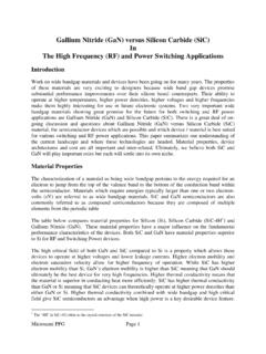
6 In either case, the devices of interest for switching and RF power applications require an epitaxial layer of either SiC or GaN to be grown or deposited on a substrate composed of either the same (homoepitaxy) or a different (heteroepitaxy) material. Homoepitaxial SiC devices are fabricated in a way that is analogous to Silicon in that a SiC epi layer is formed on a SiC substrate (Figure 1). The result is a good crystallographic match between the epi and substrate and an electrically and thermally conductive path from the top to the bottom of the wafer. This has implications on the device structures which can be fabricated as well as cost. There are a number of companies producing SiC substrate and epi wafers.
7 Cree has historically held the dominant position but other companies are closing the gap very quickly both in terms of material quality and, just as importantly, cost. Figure 1: Vertical DMOS SiC MOSFET SiC epi Microsemi PPG Page 3 GaN substrates are available today and primarily used to manufacture blue laser diodes on 2 wafers which is the current state of the art for this material2. A homoepitaxial GaN wafer offers advantages over heteroepitaxy approaches for GaN-based devices; however, production processes for epi ready GaN substrates of high quality (low defect) are still in the early stages and much less mature than SiC. Just as with SiC, there are many inherent challenges that must be addressed when it comes to the growth of bulk single crystal GaN to achieve an epi-ready substrate.
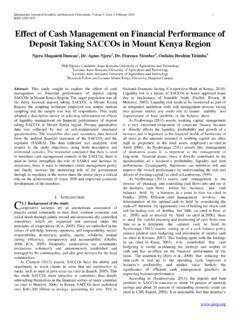
8 Therefore, the common approach today is the heteroepitaxy approach. There are several variations being implemented but for the purposes of switching and RF power applications, the primary choice today for a heteroepitaxial GaN wafer is GaN epi on a non-native SiC substrate. Another combination being used is GaN epi on Si. In both cases there are crystal lattice differences which need to be accounted for, which add additional materials and processing costs. Figure 2: Lateral MOSFET using GaN with transitional layer material to align the lattice using Si or SiC as a substrate The common approach to accomadating the crystallographic differences is through the use of a buffer layer (Figure 3).
9 Aluminum Nitride (AlN) is one material being used which provides a good material match but is electrically insulating which impacts the types of device structures which can be fabricated. Creation of the buffer layer also adds cost and process complexity. Also these buffer layers combined with the use of non-native substrates result in defects and inherent stress which need to be overcome in order to not adversely affect device performance, yields and reliability 2 Orientation Control of Bulk GaN Substrates Grown via Hydride Vapor Phase Epitaxy, Kyma Technologies, Inc. Microsemi PPG Page 4 Figure 3: Cross section of GaN and required buffer layers State-of-the-art wafer diameters are 3 going to 4 for homoepitaxial SiC and 3 for heteroepitaxy GaN on SiC or Si wafers.
10 In terms of cost, GaN on SiC wafers cost about 20% more than their SiC on SiC counterparts. From a device manufacturing point of view, defectivity for GaN on SiC or GaN on Si wafers is higher than their SiC on SiC counterparts. This is an important consideration because unlike simple diodes or LEDs, power devices are very sensitive to defects. In addition, GaN on Si has a 2 to 1 difference (Figure 4) in the coefficient of thermal expansion (CTE) at the epi interface, which can be an issue during power cycling (another reason why additional layers of material are required to make the device mechanically sound). GaN on Silicon wafers promise to be substantially lower cost than either the SiC on SiC or GaN on SiC wafers leading to a great deal of current interest in this combination.