Transcription of I2 C / SMBus High-Speed I2C Slave Purpose I/O General Pin ...
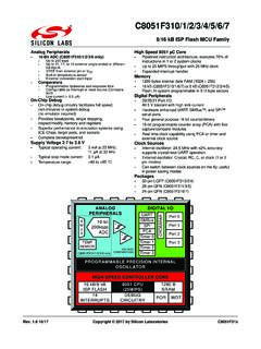
1 EFM8 Laser Bee FamilyEFM8LB1 Data SheetThe EFM8LB1, part of the Laser Bee family of MCUs, is a per-formance line of 8-bit microcontrollers with a comprehensive ana-log and digital feature set in small devices offer state-of-the-art performance by integrating 14-bit ADC, internalcalibrated temperature sensor ( 3 C), and up to four 12-bit DACs into small packages,making them ideal for the most stringent analog requirement applications. With an effi-cient, pipelined 8051 core with maximum operating frequency at 72 MHz, various com-munication interfaces, and four channels of configurable logic, the EFM8LB1 family isoptimal for many embedded applications include the following.
2 KEY FEATURES Pipelined 8-bit 8051 MCU Core with72 MHz operating frequency Up to 29 multifunction I/O pins One 14-bit, 900 ksps ADC Up to four 12-bit DACs withsynchronization and PWM capabilities Two low-current analog comparators withbuilt-in reference DACs Internal calibrated temperature sensor( 3 C) Internal 72 MHz and MHz oscillatorsaccurate to 2% Four channels of Configurable Logic 6- channel PWM / PCA Six 16-bit General - Purpose timers Optical network modules Precision instrumentation Industrial control and automation Smart sensorsI/O PortsCore / MemoryClock ManagementCIP-51 8051 Core(72 MHz)High Frequency72 MHz RC OscillatorEnergy ManagementBrown-Out Detector8-bit SFR busSerial InterfacesTimers and TriggersAnalog InterfacesSPIS ecurityPin ResetADC2 x ComparatorsInternal Voltage Reference16-bit CRCF lash Program Memory(up to 64 KB)RAM Memory(up to 4352 bytes)Debug Interface with C2 Lowest power mode with peripheral operational.
3 IdleNormalShutdownSuspendSnoozeTimer 3/4Up to 4 x Voltage DACHigh MHz RC OscillatorPin WakeupExternal InterruptsGeneral Purpose I/OI2C / SMBus2 x UARTHigh-Speed I2C SlaveExternal OscillatorLow FrequencyRC Oscillator4 x Configurable Logic UnitsWatchdog TimerPCA/PWMT imers0/1/2/5 Internal LDO RegulatorPower-On | Building a more connected 1. Feature ListThe EFM8LB1 device family are fully integrated, mixed-signal system-on-a-chip MCUs. Highlighted features are listed below. Core: Pipelined CIP-51 Core Fully compatible with standard 8051 instruction set 70% of instructions execute in 1-2 clock cycles 72 MHz maximum operating frequency Memory: Up to 64 kB flash memory (63 kB user-accessible), in-sys-tem re-programmable from firmware in 512-byte sectors Up to 4352 bytes RAM (including 256 bytes standard 8051 RAM and 4096 bytes on-chip XRAM) Power: Internal LDO regulator for CPU core voltage Power-on reset circuit and brownout detectors I/O: Up to 29 total multifunction I/O pins.
4 Up to 25 pins 5 V tolerant under bias Selectable state retention through reset events Flexible peripheral crossbar for peripheral routing 5 mA source, mA sink allows direct drive of LEDs Clock Sources: Internal 72 MHz oscillator with accuracy of 2% Internal MHz oscillator with 2% accuracy Internal 80 kHz low-frequency oscillator External CMOS clock option (up to 50 MHz) External RC oscillator (up to MHz) Analog: 14/12/10-Bit Analog-to-Digital Converter (ADC) Internal calibrated temperature sensor ( 3 C) 4 x 12-Bit Digital-to-Analog Converters (DAC) 2 x Low-current analog comparators with adjustable refer-ence Communications and Digital Peripherals: 2 x UART, up to 3 Mbaud SPI Master / Slave , up to 12 Mbps SMBus /I2C Master / Slave , up to 400 kbps I2C High-Speed Slave , up to Mbps 16-bit CRC unit, supporting automatic CRC of flash at 256-byte boundaries 4 Configurable Logic Units Timers/Counters and PWM.
5 6- channel Programmable Counter Array (PCA) supportingPWM, capture/compare, and frequency output modes 6 x 16-bit General - Purpose timers Independent watchdog timer, clocked from the low frequen-cy oscillator On-Chip, Non-Intrusive Debugging Full memory and register inspection Four hardware breakpoints, single-stepping Pre-programmed UART or SMBus bootloaderWith on-chip power-on reset, voltage supply monitor, watchdog timer, and clock oscillator, the EFM8LB1 devices are truly standalonesystem-on-a-chip solutions. The flash memory is reprogrammable in-circuit, providing nonvolatile data storage and allowing field up-grades of the firmware. The on-chip debugging interface (C2) allows non-intrusive (uses no on-chip resources), full speed, in-circuitdebugging using the production MCU installed in the final application.
6 This debug logic supports inspection and modification of memoryand registers, setting breakpoints, single stepping, and run and halt commands. All analog and digital peripherals are fully functionalwhile debugging. Device operation is specified from V up to a V supply. Devices are available in 4x4 mm 32-pin QFN, 3x3 mm24-pin QFN, 32-pin QFP, or 24-pin QSOP packages. All package options are lead-free and RoHS Data SheetFeature | Building a more connected | 22. Ordering InformationEFM8LB1 2F64EA QFN32 RTape and Reel (Optional)RevisionPackage Type S1 SMBus Bootloader (S) and Bootloader Revision (0 or 1) (Optional)Temperature Grade E (-40 to +105)Flash Memory Size 64 KBMemory Type (Flash)Family Feature SetLaser Bee 1 FamilySilicon Labs EFM8 Product LineFigure EFM8LB1 Part NumberingAll EFM8LB1 family members have the following features.
7 CIP-51 Core running up to 72 MHz Three Internal Oscillators (72 MHz, MHz and 80 kHz) SMBus I2C Slave SPI 2 UARTs 6- channel Programmable Counter Array (PWM, Clock Generation, Capture/Compare) Six 16-bit Timers Four Configurable Logic Units 14-bit Analog-to-Digital Converter with integrated multiplexer , voltage reference, temperature sensor, channel sequencer, and direct-to-XRAM data transfer Two Analog Comparators 16-bit CRC Unit Temperature range: -40 to +105 CIn addition to these features, each part number in the EFM8LB1 family has a set of features that vary across the product line. Theproduct selection guide shows the features available on each family Product Selection GuideOrdering Part NumberFlash Memory (kB)RAM (Bytes)Digital Port I/Os (Total)ADC0 ChannelsVoltage DACsComparator 0 InputsComparator 1 InputsBootloader TypeBootloader PinsPb-free (RoHS Compliant) / / Data SheetOrdering | Building a more connected | 3 Ordering Part NumberFlash Memory (kB)RAM (Bytes)Digital Port I/Os (Total)ADC0 ChannelsVoltage DACsComparator 0 InputsComparator 1 InputsBootloader TypeBootloader PinsPb-free (RoHS Compliant)
8 / / / / / / / / / / / / / / / / / / / / / / / / / / / / / Data SheetOrdering | Building a more connected | 4 Ordering Part NumberFlash Memory (kB)RAM (Bytes)Digital Port I/Os (Total)ADC0 ChannelsVoltage DACsComparator 0 InputsComparator 1 InputsBootloader TypeBootloader PinsPb-free (RoHS Compliant) / / / / / / / / / and DAC1 are enabled on devices with 2 DACs Bootloader for more information on the bootloader types and pin usage. EFM8LB1 Data SheetOrdering | Building a more connected | 5 Table of Contents1. Feature Ordering System Counters/Timers and Communications and Other Digital Reset Electrical Electrical Recommended Operating Power Reset and Supply Flash Power Management Internal External Clock External Voltage Temperature V Internal LDO Voltage Configurable Port Thermal Absolute Maximum Typical Connection Other Pin | Building a more connected | EFM8LB1x-QFN32 Pin EFM8LB1x-QFP32 Pin EFM8LB1x-QFN24 Pin EFM8LB1x-QSOP24 Pin QFN32 Package Package PCB Land Package QFP32 Package Package PCB Land Package
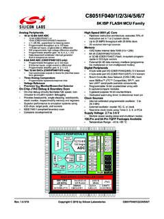
9 QFN24 Package Package PCB Land Package QSOP24 Package Package PCB Land Package Revision | Building a more connected | 73. System IntroductionSystem ClockConfigurationCIP-51 8051 ControllerCore64 KB ISP FlashProgram Memory256 Byte SRAMSFR Bus4096 Byte XRAMSYSCLKI ndependent Watchdog TimerPower NetVoltage RegulatorVDDGNDEXTCLKP ower-On ResetSupply MonitorC2CK/RSTbResetDebug / Programming HardwareC2 DAnalog PeripheralsDigital PeripheralsAMUXP riority Crossbar DecoderCrossbar ControlPort I/O ConfigurationCRC2 Comparators14/12/10-bit ADCTemp SensorVREFVDDVDDI nternal Reference+-+-UART1 Timers 0, 1, 2, 3, 4, 56-ch PCAI2C / SMBusSPIPort 0 DriversPort 1 2 3 SlaveVIOEXTOSCC onfig.
10 Logic Units (4) MHz 2% OscillatorCMOS Clock Input72 MHz 2% OscillatorLow Freq. OscillatorExternalRC Oscillator4 12-bit DACsFigure Detailed EFM8LB1 Block DiagramThis section describes the EFM8LB1 family at a high more information on the device packages and pinout, electrical specifications, and typical connection diagrams, see the EFM8LB1 Data Sheet. For more information on each module including register definitions, see the EFM8LB1 Reference Manual. For more infor-mation on any errata, see the EFM8LB1 Data SheetSystem | Building a more connected | PowerAll internal circuitry draws power from the VDD supply pin. External I/O pins are powered from the VIO supply voltage (or VDD on devi-ces without a separate VIO connection), while most of the internal circuitry is supplied by an on-chip LDO regulator.