Transcription of Introduction: The Nature of VCRs - Vishay Intertechnology
1 AN105 Siliconix10-Mar-97 1 T V e e e Introduction: The Nature of VCRsA voltage-controlled resistor (VCR) may be defined as athree-terminal variable resistor where the resistance val-ue between two of the terminals is controlled by a voltagepotential applied to the a junction field-effect transistor (JFET) under certainoperating conditions, the resistance of the drain-sourcechannel is a function of the gate-source voltage alone andthe JFET will behave as an almost pure ohmic drain-source current, IDSS, and minimum re-sistance rDS(on), will exist when the gate-source voltageis equal to zero volts (VGS = 0). If the gate voltage is in-creased (negatively for n-channel JFETs and positivelyfor p-channel), the resistance will also increase. When thedrain current is reduced to a point where the FET is nolonger conductive, the maximum resistance is voltage at this point is referred to as the pinchoff orcutoff voltage and is symbolized by VGS = VGS(off).
2 Thusthe device functions as a voltage- controlled 1 Region 2ID Current Saturation Region Ohmic Region %# %"& D D D" ( %" $ D" %"" $ ID e '! ( E ! " $ " $ " #$ #Figure 1 details typical operating characteristics of an n-channel JFET. Most amplification or switching operationsof FETs occur in the constant-current (saturated) region,shown as Region II. A close inspection of Region I (the un-saturated or pre-pinchoff area) reveals that the effectiveslope indicative of conductance across the channel fromdrain-to-source is different for each value of gate-sourcebias voltage. The slope is relatively constant over a range ofapplied drain voltages, so long as the gate voltage is alsoconstant and the drain voltage is Properties of FETsThe unique resistance-controlling properties of FETs canbe deduced from Figure 2, which is an expanded-scaleplot of the encircled area in the lower left-hand corner ofFigure 1.))
3 The output characteristics all pass through theorigin, near which they become almost straight lines sothat the incremental value of channel resistance, rDS, isessentially the same as that of dc resistance, rDS, and is afunction of 2 shows an extension of the operating characteris-tics into the third quadrant for a typical n-channel such devices are normally operated with a positivedrain-source voltage, small negative values of VDS arepossible. This is because the gate-channel PN junctionmust be slightly forward-biased before any significantamount of gate current flows. The slope of the VGS biasline is equal to ID/VDS = 1/rDS. This value is controlledby the amount of voltage applied to the gate. MinimumrDS, usually expressed as rDS(on), occurs at VGS = 0 andis dictated by the geometry of the FET. A device with achannel of small cross-sectional area will exhibit a highrDS(on) and a low IDSS. Thus a FET with high IDSS shouldbe chosen where design requirements indicate the needfor a low rDS(on).
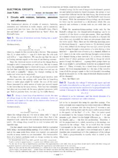
4 Updates to this app note may be obtained via facsimile by calling Siliconix FaxBack, 1-408-970-5600. Please request FaxBack document # 2 Siliconix10-Mar-97 400 200200400 VGS = V2000 V VDGSIDVGS = 0 V V V(IDA) VDS (V)(mA)ID321510 VVDS (mV)0 V VFigure2 N Channel JFET Output CharacteristicsEnlarged Around VDS=0V V VVGS = V 200 The graph in Figure 3 is useful in estimating rDS valuesat any given value of VGS. The resistance is normalizedto its specific value at VGS = 0 V. The dynamic range ofrDS is shown as greater than 100:1, although for best con-trol of rDS a range of 10:1 is normally rDS Data/rDS(on)() rDSVGS/VGS(off) VrDS]rDS(on)1 VGS VGS(off)Siliconix offers a family of n-channel FETs specificallyintended for use as voltage-controlled resistors. These de-vices have rDS(on) values ranging from 20 to 4,000 ,where VCR2N = 20 60 , VCR4N = 200 600 ,VCR7N = 4 k 8 k .Applications for VCRsA simple application of a FET VCR is shown in Figure 4,the circuit for a voltage divider + Figure Attenuator CircuitThe output voltage is:VOUT+VINrDSR)rDS(1)It is assumed that the output voltage is not so large as topush the VCR out of the linear resistance region, and thatthe rDS is not shunted by the lowest value which vOUTcan assume is:VOUT(min)+VINrDS(on)R)rDS(on)(2)Signa l Distortion: CausesFigure 2 shows that the bias lines bend down as VDSincreases in a positive direction toward the pinch-off voltageof the FET.
5 The bending of the bias lines results in a changein rDS, and hence the distortion encountered in VCR circuits;note that the distortion occurs in both the first and thirdquadrants. Distortion results because the channel depletionlayer increases as VDS reduces the drain current so that apinch-off condition is reached when VDS = VGS VGS(off).Figure 5 shows how the current has an opposite effect in thethird quadrant, increasing negatively with an increasinglynegative VDS. This is due to the forward conduction of thegate-to-channel junction when the drain signal exceeds thenegative gate bias 3 VOUTVINVCRVGSR+ GDiodeAnodeDiodeCathodewhen SignalSwings Negative+V V0 Figure Attenuator CircuitVOUTVINVCRVGGR1+ R3R2 VCR LinearizationR2 = R3 // 10(rDS//Rload//R1)Figure +VCONTROLF igure Signal DistortionThe majority of VCR applications require that signaldistortion be kept to a minimum. Also, numerousapplications require large signal handling capability.
6 Asimple feedback technique may be used to reducedistortion while permitting large signal handlingcapability; a small amount of drain signal is coupled to thegate through a resistor divider network, as shown inFigure application of a part of the positive drain signal to thegate causes the channel depletion layer to decrease, witha corresponding increase in drain current. Increasing thedrain current for a given drain voltage tends to linearizethe VGS bias curves. On the negative half-cycle, a smallnegative voltage is coupled to the gate to reduce theamount of drain-gate forward bias. This in turn reducesthe drain current and linearizes the bias lines. Now thechannel resistance is dependent on the dc gate controlvoltage and not on the drain signal, unless the VDS = VGS VGS(off) locus is approached. Resistors R2 and R3 inFigure 6 couple the drain signal to the gate; the resistorvalues are equal, so that symmetrical voltage-currentcharacteristics are produced in both quadrants.
7 Theresistors must be sufficiently large to provide minimumloading to the circuit:R2 = R3 w 10 [R1 rDS (max) RL](3)Typically, 470-k resistors will work well for most ap-plications. R1 is selected so that the ratio of rDS(on) RL to[(rDS(on) RL) + R1] give the desired output voltage, or:VO+VIrDS(on) RL(rDS(on) RL))R1(4)The feedback technique used in Figure 6 requires that thegate control voltage, VGG, be twice as large as VGS in Fig-ure 5 for the same rDS value. Use of a floating supply be-tween the resistor junction and the FET gate will over-come this problem. The circuit is shown in Figure 7 andallows the gate control voltage to be the same value as thatvoltage used without a feedback circuit, while preservingthe advantages to be gained through the feedback 4 Siliconix10-Mar-97 Experimental ResultsFigures 8 and 9 show low voltage output characteristiccurves for a typical Siliconix n-channel voltage-controlledresistor, VCR7N.
8 Bias conditions are shown both with andwithout feedback. Figure 8 shows a two-volt peak-to-peaksignal on the VGS = 0 V bias curve, with the VCR operatingin the first and third quadrants. The VCR is operated forward-biased gate-drain PN junction may be seenat approximately V, and bending of the bias curve isapparent in the third quadrant. The photo also demon-strates the comparison between a fixed resistor (the linearline superimposed on the bias curve) and the distortionapparent in the VCR without feedback compensation; theVCR signal is unusable with the indicated amount of dis-tortion at 2 V Figure 9, the same VCR7N FET is shown operatingwith the addition of the feedback resistors. Distortion hasbeen reduced to less than , and the characteristics ofthe VCR are now closely comparable to those of a Figures 8 and 9, the same VCR FET characteristics areshown, with VGS adjusted for higher rDS. No feedbacknetwork is employed in Figure 8, and measured distortionis greater than 8%.
9 In Figure 9, the feedback resistorshave been added and distortion has been reduced to lessthan degree of non-linearity will be experienced in boththe first and third quadrants as VGS approaches the FETcut-off voltage. For this reason, it is important that thefeedback resistors be of equal value so that the non-linear-ities likewise will be equal in both 100 200 = VCONTROLVGS = 0 VVGS = V2001000 100 200 = VCONTROL = 0 VVGS = 3 VVCONTROL = 6 VFigure Without FeedbackFigure With Feedback. Drain Current (IDA)m Drain Current (IDA)mVDS Drain-Source Voltage (V)VDS Drain-Source Voltage (V) 1: Distortion vs. TemperatureTemperatureWithout FeedbackWith FeedbackTemperature( C)rDS = rDS(on)rDS = 10 rDS(on)rDS = rDS(on)rDS = 10 rDS(on)+125>13%>6%< < +25>10%>5%< < < < 5 Distortion resulting from changes in temperature is alsominimized by the feedback resistor technique. On-resis-tance will change with temperature in an inverse mannerto the behavior of FET drain current.
10 Table 1 presents theresult of VCR laboratory performance tests of distortionversus temperature. The VCR7N again was level was 2 V application note has presented a brief description of theuse of junction field-effect transistors as voltage-controlledresistors, including details of operation, characteristics, li-mitations, and applications. The VCR is capable of opera-tion as a symmetrical resistor with no dc bias voltage in thesignal loop, an ideal characteristic for many large signal-handling capability and minimumdistortion are system requirements, the feedback neutral-ization technique for VCRs is an important tool in achiev-ing either or both has also been shown that FETs with high pinch-off volt-age require larger drain-to-source voltages to producedrain current saturation. Therefore, FETs with highVGS(off) will have a larger dynamic range in terms of ap-plied signal amplitude, while maintaining a linear resis-tance.