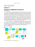
Transcription of IR Receiver Modules for Remote Control Systems
1 , Semiconductors Rev. , 26-Sep-20181 Document Number: 82463 THIS DOCUMENT IS SUBJECT TO CHANGE WITHOUT NOTICE. THE PRODUCTS DESCRIBED HEREIN AND THIS DOCUMENTARE SUBJECT TO SPECIFIC DISCLAIMERS, SET FORTH AT Receiver Modules for Remote Control SystemsDESIGN SUPPORT TOOLSMECHANICAL DATAP inning1 = GND, 2 = , 3 = VS, 4 = OUTORDERING - top view - side view tapedFEATURES Improved immunity against HF and RF noise Low supply current Photo detector and preamplifier in one package Internal filter for PCM frequency Supply voltage: V to V Improved immunity against optical noise Insensitive to supply voltage ripple and noise Taping available for top view and side view assembly Material categorization: for definitions of compliance please see series are miniaturized SMD IR Receiver Modules for infrared Remote Control Systems . A PIN diode and a preamplifier are assembled on a leadframe, the epoxy package contains an IR demodulated output signal can be directly connected to a microprocessor for series devices are optimized to suppress almost all spurious pulses from Wi-Fi and CFL sources.
2 They may suppress some data signals if continuously series devices are provided primarily for compatibility with old AGC2 designs. New designs should prefer the series containing the newer components have not been qualified according to automotive logo to get startedAvailableModelsPARTS TABLEAGCLEGACY, FORLONG BURST Remote CONTROLS (AGC2)RECOMMENDED FORLONG BURST CODES (AGC4)Carrier frequency30 kHzTSOP6230 TSOP643033 kHzTSOP6233 TSOP643336 kHzTSOP6236 TSOP6436 (1)(2)(3)38 kHzTSOP6238 TSOP6438 (4)(5)40 kHzTSOP6240 TSOP644056 kHzTSOP6256 TSOP6456 (6)(7)PackagePanheadPinning1 = GND, 2 = , 3 = VS, 4 = OUTD imensions (mm) W x H x DMountingSMDA pplicationRemote controlBest choice for(1) RC-5 (2) RC-6 (3) Panasonic (4) NEC (5) Sharp (6) r-step (7) Thomson , Semiconductors Rev. , 26-Sep-20182 Document Number: 82463 THIS DOCUMENT IS SUBJECT TO CHANGE WITHOUT NOTICE. THE PRODUCTS DESCRIBED HEREIN AND THIS DOCUMENTARE SUBJECT TO SPECIFIC DISCLAIMERS, SET FORTH AT DIAGRAMAPPLICATION CIRCUITNote Stresses beyond those listed under Absolute Maximum Ratings may cause permanent damage to the device.
3 This is a stress rating only and functional operation of the device at these or any other conditions beyond those indicated in the operational sections of this specification is not implied. Exposure to absolute maximum rating conditions for extended periods may affect the device reliability33 k VSOUTDemo-GNDpassAGCI nputPINB anddulatorControl circuit34116839-1C1IR receiverGNDC ircuit CR1+ VSGNDT ransmitterwithTSAL xxxxVSVO17170-11 OUTR1 and C1 recommended to reduce supply ripple for VS < VABSOLUTE MAXIMUM RATINGSPARAMETERTEST CONDITIONSYMBOLVALUEUNITS upply to +6 VSupply currentIS5mAOutput to (VS + )VOutput currentIO5mAJunction temperatureTj100 CStorage temperature rangeTstg-25 to +85 COperating temperature rangeTamb-25 to +85 CPower consumptionTamb 85 CPtot10mWELECTRICAL AND OPTICAL CHARACTERISTICS (Tamb = 25 C, unless otherwise specified)PARAMETERTEST currentVS = 5 V, Ev = = 40 klx, distanceEv = 0,IR diode TSAL6200, IF = 50 mA,test signal see Fig.
4 1d-18-mOutput voltage lowIOSL = mA, Ee = mW/m2,test signal see Fig. 1 VOSL--100mVMinimum irradiancePulse width tolerance:tpi - 5/fo < tpo < tpi + 6/fo,test signal see Fig. 1Ee irradiancetpi - 5/fo < tpo < tpi + 6/fo,test signal see Fig. 1Ee of half transmission distance 1/2- 50- , Semiconductors Rev. , 26-Sep-20183 Document Number: 82463 THIS DOCUMENT IS SUBJECT TO CHANGE WITHOUT NOTICE. THE PRODUCTS DESCRIBED HEREIN AND THIS DOCUMENTARE SUBJECT TO SPECIFIC DISCLAIMERS, SET FORTH AT CHARACTERISTICS (Tamb = 25 C, unless otherwise specified)Fig. 1 - Output Active LowFig. 2 - Pulse Length and Sensitivity in Dark AmbientFig. 3 - Output FunctionFig. 4 - Output Pulse DiagramFig. 5 - Frequency Dependence of ResponsivityFig. 6 - Sensitivity in Bright Ambient16110 EeTtpi *t* tpi10/f0 is recommended for optimal functionVOVOHVOLtOptical Test Signal(IR diode TSAL6200, IF = A, 30 pulses, f = f0, t = 10 ms)Output Signaltd1)tpo2)1) 7/f0 < td < 15/f02) tpi - 5/f0 < tpo < tpi + 6 - Irradiance (mW/m2)tpo - Output Pulse Width (ms)Input burst lengthOutput pulse width = 950 nm,optical test signal, s600 st = 60 mstontoff94 8134 Optical Test SignalOutput Signal, (see Fig.
5 4)0 1 10 100 1000 10 000 ton, toff - Output Pulse Width (ms) Ee - Irradiance (mW/m2) ton toff = 950 nm,optical test signal, fig. 1 - Relative Frequency16925f = f0 5 % f(3 dB) = f0/10Ee - Relative - Ambient DC Irradiance (W/m2)Ee min. - Threshold Irradiance (mW/m2)Correlation with ambient light sources:10 W/m2 = klx (std. illum. A, T = 2855 K)10 W/m2 = klx (daylight, T = 5900 K) Wavelength of ambient illumination: = 950 , Semiconductors Rev. , 26-Sep-20184 Document Number: 82463 THIS DOCUMENT IS SUBJECT TO CHANGE WITHOUT NOTICE. THE PRODUCTS DESCRIBED HEREIN AND THIS DOCUMENTARE SUBJECT TO SPECIFIC DISCLAIMERS, SET FORTH AT 7 - Sensitivity vs. Supply Voltage DisturbancesFig. 8 - Max. Envelope Duty Cycle vs. Burst LengthFig. 9 - Sensitivity vs. Ambient TemperatureFig. 10 - Relative Spectral Sensitivity vs. WavelengthFig.
6 11 - Horizontal DirectivityFig. 12 - Sensitivity vs. Supply VsRMS - AC Voltage on DC Supply Voltage (mV)Ee min. - Threshold Irradiance (mW/m2)f = f0f = 20 kHzf = 30 kHzf = 100 Hzf = 10 Length (Number of Cycles/Burst)Max. Envelope Duty Cyclef = 38 kHz, Ee = 2 mW/m - Ambient Temperature ( C)Ee min. - Sensitivity (mW/m2) Title1st line2nd line2nd lineS( ) Relative Spectral Sensitivity - Wavelength (nm) 30 10 20 40 50 60 70 80 Relative Transmission - Supply Voltage (V)Ee min. - Sensitivity (mW/m2) , Semiconductors Rev. , 26-Sep-20185 Document Number: 82463 THIS DOCUMENT IS SUBJECT TO CHANGE WITHOUT NOTICE. THE PRODUCTS DESCRIBED HEREIN AND THIS DOCUMENTARE SUBJECT TO SPECIFIC DISCLAIMERS, SET FORTH AT DATA FORMATThis series is designed to suppress spurious output pulses due to noise or disturbance signals. The devices can distinguish data signals from noise due to differences in frequency, burst length, and envelope duty cycle.
7 The data signal should be close to the device s band-pass center frequency ( 38 kHz) and fulfill the conditions in the table a data signal is applied to the product in the presence of a disturbance, the sensitivity of the Receiver is automatically reduced by the AGC to insure that no spurious pulses are present at the Receiver s examples which are suppressed are: DC light ( from tungsten bulbs sunlight) Continuous signals at any frequency Strongly or weakly modulated noise from fluorescent lamps with electronic ballasts (see Fig. 13 or Fig. 14) GHz and 5 GHz Wi-Fi Fig. 13 - IR Disturbance from Fluorescent LampWith Low ModulationFig. 14 - IR Disturbance from Fluorescent LampWith High ModulationNote For data formats with short bursts please see the datasheet of , , Title1st line2nd line2nd lineIR Signal AmplitudeTime (ms)1692110100100010000-60-40-2002040051 01520 Axis Title1st line2nd line2nd lineIR Signal AmplitudeTime (ms) burst length10 cycles/burst10 cycles/burstAfter each burst of length a minimum gap time is required of10 to 70 cycles 12 cycles10 to 35 cycles 12 cyclesFor bursts greater than a minimum gap time in the data stream is needed of70 cycles> 4 x burst length35 cycles> 10 x burst lengthMaximum number of continuous short bursts/second8001300 NEC codeYesPreferredRC5 / RC6 codeYesPreferredThomson 56 kHz codeYesPreferredSharp codeYesPreferredSuppression of interference from fluorescent lampsMild disturbance patternsare suppressed (example:signal pattern of Fig.)
8 13)Complex and critical disturbance patternsare suppressed (example: signal patternof Fig. 14 or highly dimmed LCDs) , Semiconductors Rev. , 26-Sep-20186 Document Number: 82463 THIS DOCUMENT IS SUBJECT TO CHANGE WITHOUT NOTICE. THE PRODUCTS DESCRIBED HEREIN AND THIS DOCUMENTARE SUBJECT TO SPECIFIC DISCLAIMERS, SET FORTH AT DIMENSIONS in millimetersASSEMBLY INSTRUCTIONSR eflow Soldering Reflow soldering must be done within 72 h while stored under a max. temperature of 30 C, 60 % RH after opening the dry pack envelope Set the furnace temperatures for pre-heating and heating in accordance with the reflow temperature profile as shown in the diagram. Exercise extreme care to keep the maximum temperature below 260 C. The temperature shown in the profile means the temperature at the device surface. Since there is a temperature difference between the component and the circuit board, it should be verified that the temperature of the device is accurately being measured Handling after reflow should be done only after the work surface has been cooled offManual Soldering Use a soldering iron of 25 W or less.
9 Adjust the temperature of the soldering iron below 300 C Finish soldering within 3 s Handle products only after the temperature has cooled x = and place area. TR x = to DINtechnical drawingsNot indicated tolerances and place area. TT tapingFootprint( )( )Issue: 8; : , Semiconductors Rev. , 26-Sep-20187 Document Number: 82463 THIS DOCUMENT IS SUBJECT TO CHANGE WITHOUT NOTICE. THE PRODUCTS DESCRIBED HEREIN AND THIS DOCUMENTARE SUBJECT TO SPECIFIC DISCLAIMERS, SET FORTH AT LEAD (Pb)-FREE REFLOW SOLDER PROFILETAPING VERSION DIMENSIONS in millimetersmax. 120 smax. 100 smax. 20 sMax. ramp up 3 C/smax. 260 C101001000100000501002503000300 Axis Title2nd lineTemperature ( C)Time (s)25020015010050200150245 C217 C240 C255 CMax. ramp down 6 C/sMax. 2 cycles , Semiconductors Rev. , 26-Sep-20188 Document Number: 82463 THIS DOCUMENT IS SUBJECT TO CHANGE WITHOUT NOTICE. THE PRODUCTS DESCRIBED HEREIN AND THIS DOCUMENTARE SUBJECT TO SPECIFIC DISCLAIMERS, SET FORTH AT VERSION DIMENSIONS in , Semiconductors Rev.
10 , 26-Sep-20189 Document Number: 82463 THIS DOCUMENT IS SUBJECT TO CHANGE WITHOUT NOTICE. THE PRODUCTS DESCRIBED HEREIN AND THIS DOCUMENTARE SUBJECT TO SPECIFIC DISCLAIMERS, SET FORTH AT DIMENSIONS in millimetersLEADER AND TRAILER DIMENSIONS in millimetersCOVER TAPE PEEL STRENGTHA ccording to DIN EN N to N300 mm/min. 10 to 180 peel angleLABELS tandard bar code labels for finished goodsThe standard bar code labels are product labels and used for identification of goods. The finished goods are packed in final packing area. The standard packing units are labeled with standard bar code labels before transported as finished goods to warehouses. The labels are on each packing unit and contain vishay Semiconductor GmbH specific 400 StartEnddevices96 11818no , Semiconductors Rev. , 26-Sep-201810 Document Number: 82463 THIS DOCUMENT IS SUBJECT TO CHANGE WITHOUT NOTICE. THE PRODUCTS DESCRIBED HEREIN AND THIS DOCUMENTARE SUBJECT TO SPECIFIC DISCLAIMERS, SET FORTH AT PACKINGThe reel is packed in an anti-humidity bag to protect the devices from absorbing moisture during transportation and PACKINGThe sealed reel is packed into a cardboard METHOD OF STORAGEDry box storage is recommended as soon as the aluminum bag has been opened to prevent moisture absorption.