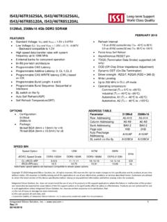
Transcription of IS31FL3733 - ISSI
1 IS31FL3733 . 12 16 DOTS MATRIX LED DRIVER. WITH INDIVIDUAL AUTO BREATH FUNCTION. January 2017. GENERAL DESCRIPTION FEATURES. The IS31FL3733 is a general purpose 12 16 LEDs Supply voltage range: to matrix driver with 1/12 cycle rate. The device can be 16 current source outputs for row control programmed via an I2C compatible interface. Each 12 switch current inputs for column scan control LED can be dimmed individually with 8-bit PWM data Up to 192 LEDs (12 16) in dot matrix which allowing 256 steps of linear dimming. Programmable 12 16 (64 RGBs) matrix size with IS31FL3733 features 3 Auto Breathing Modes which de-ghost function are noted as ABM-1, ABM-2 and ABM-3. For each 1 MHz I2C-compatible interface Auto Breathing Mode, there are 4 timing characters Selectable 3 Auto Breath Modes for each dot which include current rising / holding / falling / off time and 3 loop characters which include Loop-Beginning / Auto Breath Loop Features interrupt pin inform Loop-Ending / Loop-Times.
2 Every LED can be MCU Auto Breath Loop completed configured to be any Auto Breathing Mode or No- Auto Breath offers 128 steps gamma current, Breathing Mode individually. interrupt and state look up registers 256 steps Global Current Setting Additionally each LED open and short state can be detected, IS31FL3733 store the open or short Individual on/off control information in Open-Short Registers. The Open-Short Individual 256 PWM control steps Registers allowing MCU to read out via I2C Individual Auto Breath Mode select compatible interface. Inform MCU whether there are Individual open and short error detect function LEDs open or short and the locations of open or short Cascade for synchronization of chips LEDs. QFN-48 (6mm 6mm) and eTQFP-48 packages The IS31FL3733 operates from to and features a very low shutdown and operational current. APPLICATIONS. IS31FL3733 is available in QFN-48 (6mm 6mm) and Mobile phones and other hand-held devices for eTQFP-48 packages.
3 It operates from to LED display over the temperature range of -40 C to +125 C. Gaming device (Keyboard, Mouse etc.). LED in white goods application TYPICAL APPLICATION CIRCUIT. VBattery VIO/MCU. *Note 2 20 39. PVCC VIO. 22 F/10V F F F. 29. PVCC CS1 CS2 CS3 CS4 CS5 CS6 CS7 CS8 CS9 CS10 CS11 CS12 CS13 CS14 CS15 CS16. F F. 37 AVCC 33. CS16 L. 38 DVCC 32 SW12. F F CS15. K. SW11. VIO/MCU J. SW10. 17. 100k 1k 1k CS2 I. 16 SW9. 41 CS1. SDA H. 42 SW8. Micro SCL IS31FL3733 . 45 G. Controller INTB 15 SW7. 46 SW12. SDB 14 F. 47 SW11 SW6. IICRST. 100k 100k E. SW5. D. 3 SW4. 40 SW2. SYNC 2 C. 35 SW1 SW3. RSET. 43 B. REXT ADDR1 SW2. 20k 44 5,12. ADDR2 PGND A. 48 34 SW1. GND AGND. 1 2 3 4 5 6 7 8 9 10 11 12 13 14 15 16. Figure 1 Typical Application Circuit (12 16). Integrated Silicon Solution, Inc. 1. Rev. B, 12/20/2016. IS31FL3733 . TYPICAL APPLICATION CIRCUIT (CONTINUED). VBattery VIO/MCU. *Note 2 20 39. PVCC VIO. 22 F/10V F F F. 29. PVCC CS1 CS2 CS3 CS4 CS5 CS6 CS7 CS8 CS9 CS10 CS11 CS12 CS13 CS14 CS15 CS16.
4 F F. 37 AVCC 33. CS16 L. 38 DVCC 32 SW12. F F CS15. K. SW11. VIO/MCU. J. SW10. 100k 1k 1k 17. CS2 I. 41 16 SW9. SDA CS1. 42 H. SCL SW8. Micro 45 IS31FL3733 . INTB G. Controller 46 15 SW7. SDB SW12. 47 14 F. IICRST SW11 SW6. 100k 100k E. SW5. D. 3 SW4. 40 SW2. SYNC 2 C. 35 SW1 SW3. RSET. 43 B. REXT ADDR1 SW2. 20k 44 5,12. ADDR2 PGND A. 48 34 SW1. GND AGND. 1 2 3 4 5 6 7 8 9 10 11 12 13 14 15 16. Figure 2 Typical Application Circuit (RGB). Note 1: For the mobile applications the IC should be placed far away from the mobile antenna in order to prevent the EMI. Note 2: Electrolytic/Tantalum Capacitor may considerable for high current application to avoid audible noise interference. VBattery ADDR1 ADDR1 SDA ADDR1 SCL ADDR1. ADDR2 ADDR2 ADDR2 ADDR2. VIO. 100k 1k 1k SDA. SDA SDA SDA SDA SDA SDA SDA. SCL. Micro SCL SCL SCL SCL SCL SCL SCL. INTB. Controller INTB INTB INTB INTB. SDB. SDB SDB SDB SDB SDB SDB SDB. IICRST. 100k 100k IICRST IICRST IICRST IICRST IICRST IICRST IICRST.
5 SYNC SYNC SYNC SYNC. Master Slave 1 Slave 2 Slave 3. VBattery SYNC VBattery SYNC VBattery SYNC VBattery SYNC. ADDR2 ADDR2 ADDR2 ADDR2. ADDR1 ADDR1 SDA ADDR1 SCL ADDR1. IICRST IICRST IICRST IICRST IICRST IICRST IICRST IICRST. SDA SDA SDA SDA SDA SDA SDA SDA. SCL SCL SCL SCL SCL SCL SCL SCL. INTB INTB INTB INTB. SDB SDB SDB SDB SDB SDB SDB SDB. Slave 4 Slave 5 Slave 6 Slave 7. Figure 3 Typical Application Circuit (Eight Parts Synchronization-Work). Note 3: One part is configured as master mode, all the other 7 parts configured as slave mode. Work as master mode or slave mode specified by Configuration Register (Function register, address 00h). Master part output master clock, and all the other parts which work as slave input this master clock. Integrated Silicon Solution, Inc. 2. Rev. B, 12/20/2016. IS31FL3733 . PIN CONFIGURATION. Package Pin Configuration (Top View). QFN-48. eTQFP-48. Integrated Silicon Solution, Inc. 3. Rev. B, 12/20/2016.
6 IS31FL3733 . PIN DESCRIPTION. No. Pin Description 1,36 NC Not connect. 2~4,6~11, SW1~SW12 Switch pin for LED matrix scanning. 13~15. 5,12 PGND Power GND. 16~19, 21~28, CS1~CS16 Current Source. 30~33. 20, 29 PVCC Power for current source. 34 AGND Analog GND. Input terminal used to connect an external resistor. 35 RSET. This regulates current source DC current value. 37 AVCC Power for analog circuits. 38 DVCC Power for digital circuits. 39 VIO Input logic reference voltage. Synchronize pin. It is used for more than one part 40 SYNC. work synchronize. If it is not used please float this pin. 41 SDA I2C compatible serial data. 42 SCL I2C compatible serial clock. 43 ADDR1 I2C address setting. 44 ADDR2 I2C address setting. Interrupt output pin. Register F0h sets the function of the INTB pin and active low when the interrupt event 45 INTB. happens. Can be NC (float) if interrupt function no used. 46 SDB Shutdown the chip when pull to low. Reset I2C when pull high, need to pull down when 47 IICRST.
7 Normal operation. 48 GND Connect to GND. Thermal Pad Need to connect to GND pins. Integrated Silicon Solution, Inc. 4. Rev. B, 12/20/2016. IS31FL3733 . ORDERING INFORMATION. Industrial Range: -40 C to +125 C. Order Part No. Package QTY. IS31FL3733 -QFLS4-TR QFN-48, Lead-free 2500/Reel IS31FL3733 -TQLS4 eTQFP-48, Lead-free 250/Tray Copyright 2016 Integrated Silicon Solution, Inc. All rights reserved. ISSI reserves the right to make changes to this specification and its products at any time without notice. ISSI assumes no liability arising out of the application or use of any information, products or services described herein. Customers are advised to obtain the latest version of this device specification before relying on any published information and before placing orders for products. Integrated Silicon Solution, Inc. does not recommend the use of any of its products in life support applications where the failure or malfunction of the product can reasonably be expected to cause failure of the life support system or to significantly affect its safety or effectiveness.
8 Products are not authorized for use in such applications unless Integrated Silicon Solution, Inc. receives written assurance to its satisfaction, that: a.) the risk of injury or damage has been minimized; b.) the user assume all such risks; and c.) potential liability of Integrated Silicon Solution, Inc is adequately protected under the circumstances Integrated Silicon Solution, Inc. 5. Rev. B, 12/20/2016. IS31FL3733 . ABSOLUTE MAXIMUM RATINGS. Supply voltage, VCC ~ + Voltage at any input pin ~ VCC+ Maximum junction temperature, TJMAX 150 C. Storage temperature range, TSTG -65 C ~ +150 C. Operating temperature range, TA -40 C ~ +125 C. Thermal resistance, junction to ambient, JA (QFN) 30 C/W. JA (eTQFP) 29 C/W. ESD (HBM) 8kV. ESD (CDM) 1kV. Note: Stresses beyond those listed under Absolute Maximum Ratings may cause permanent damage to the device. These are stress ratings only and functional operation of the device at these or any other condition beyond those indicated in the operational sections of the specifications is not implied.
9 Exposure to absolute maximum rating conditions for extended periods may affect device reliability. ELECTRICAL CHARACTERISTICS. The following specifications apply for VCC = , TA = 25 C, unless otherwise noted. Symbol Parameter Conditions Min. Typ. Max. Unit VCC Supply voltage V. ICC Quiescent power supply current VSDB = VCC, all LEDs off 2 3 mA. VSDB = 0V 2 5. ISD Shutdown current VSDB = VCC, Configuration Register A. 2 5. written 0000 0000. Maximum constant current of IOUT RSET=20k 38 42 46 mA. CS1~CS16. Average current on each LED RSET=20k , GCC=255, ILED mA. ILED = PWM = 255. Current sink headroom voltage ISINK = 672mA (Note 1,2) 300 400. SW1~SW12. VHR mV. Current source headroom voltage ISOURCE = 42mA (Note 1) 150 200. CS1~C16. tSCAN Period of scanning 115 128 140 s Non-overlap blanking time during tNOL scan, the SWy and CSx are all off 8 s during this time Logic Electrical Characteristics (SDA, SCL, ADDR1, ADDR2, SYNC, SDB). VIL Logic 0 input voltage VIO= GND V.
10 VIH Logic 1 input voltage VIO= VIO V. VHYS Input Schmitt trigger hysteresis VIO= V. VOL Logic 0 output voltage for SYNC IOL = 8mA V. VOH Logic 1 output voltage for SYNC IOH = 8mA V. IIL Logic 0 input current VINPUT = 0V (Note 3) 5 nA. IIH Logic 1 input current VINPUT = VIO (Note 3) 5 nA. Integrated Silicon Solution, Inc. 6. Rev. B, 12/20/2016. IS31FL3733 . DIGITAL INPUT SWITCHING CHARACTERISTICS (NOTE 3). Fast Mode Fast Mode Plus Symbol Parameter Units Min. Typ. Max. Min. Typ. Max. fSCL Serial-clock frequency - 400 - 1000 kHz Bus free time between a STOP and a START. tBUF - - s condition tHD, STA Hold time (repeated) START condition - - s tSU, STA Repeated START condition setup time - - s tSU, STO STOP condition setup time - - s tHD, DAT Data hold time - - - - s tSU, DAT Data setup time 100 - 50 - ns tLOW SCL clock low period - - s tHIGH SCL clock high period - - s Rise time of both SDA and SCL signals, tR - 300 - 120 ns receiving Fall time of both SDA and SCL signals, tF - 300 - 120 ns receiving Note 1: In case of REXT = 20k , Global Current Control Register (PG3, 01h) written 1111 1111 , GCC = 1111 1111.