Transcription of Memory Basics - Michigan State University
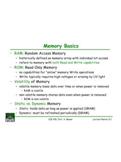
1 Memory Basics RAM: Random Access Memory historically defined as Memory array with individual bit access refers to Memory with both Read and Write capabilities ROM: Read Only Memory no capabilities for online Memory Write operations Write typically requires high voltages or erasing by UV light Volatility of Memory volatile Memory loses data over time or when power is removed RAM is volatile non-volatile Memory stores date even when power is removed ROM is non-volatile Static vs. Dynamic Memory Static: holds data as long as power is applied (SRAM). Dynamic: will lose data unless refreshed periodically (DRAM). ECE 331, Prof. A. Mason Memory SRAM/DRAM Basics SRAM: Static Random Access Memory WL. Static: holds data as long as power is applied Volatile: can not hold data if power is removed 3 Operation States: hold, write, read Basic 6T (6 transistor) SRAM Cell MAL MAR. bistable (cross-coupled) INVs for storage access transistors MAL & MAR.
2 Bit bit word line, WL, controls access WL = 0 (hold) = 1 (read/write). DRAM: Dynamic Random Access Memory Dynamic: must be refreshed periodically Volatile: loses data when power is removed 1T DRAM Cell single access transistor; storage capacitor control input: word line (WL); data I/O: bit line DRAM to SRAM Comparison DRAM is smaller & less expensive per bit SRAM is faster DRAM requires more peripheral circuitry ECE 331, Prof. A. Mason Memory ROM/PROM Basics ROM: Read Only Memory no capabilities for online Memory Write operations data programmed during fabrication: ROM. with high voltages: PROM. by control logic: PLA. Non-volatile: data stored even when power is removed PROM: Programmable Read Only Memory programmable by user -using special program tools/modes read only Memory -during normal use non-volatile Read Operation like any ROM: address bits select output bit combinations Write Operation EPROM device typically requires high voltage (~15V) control inputs to set data structure stores charge to floating gate (see figure) to set to Hi or Low Erase Operation to change data EPROM: erasable PROM: uses UV light to reset all bits EEPROM: electrically-erasable PROM, erase with control voltage ECE 331, Prof.
3 A. Mason Memory Comparison of Memory Types DRAM. very high density cheap data cache in computers must be periodically refreshed slower than SRAM. volatile; no good for program (long term) storage SRAM (basically a Latch). fastest type of Memory low density more expensive generally used in small amounts (L2 cache) or expensive servers EEPROM. slow/complex to write not good for fast cache non-volatile; best choice for program Memory ROM. hardware coded data; rarely used except for bootup code Register (flip flop). functionally similar to SRAM but less dense (and thus more expensive). reserved for data manipulation applications ECE 331, Prof. A. Mason Memory Memory Arrays N x n array of 1-bit cells Memory size : # bytes = N, # bits = N n n = byte width ; 8, 16, 32, etc. Example: N = number of bytes = length 1k x 8 RAM 10 addr lines, 8-bit bytes m = number of address bits 210 = 1k (1024) mem locations = length max N = 2m width = 8-bit, size = 1k-byte, 8k-bits Array I/O Control Data I/O.
4 Data (in and out). Dn-1 - D0. address Am-1 - A0 Address control varies with design WE = write enable (assert low). WE=1=read, WE=0=write En = block enable (assert low). used as chip enable (CE) for an SRAM chip ECE 410, Prof. A. Mason Memory Memory Array Addressing Standard Memory Addressing Scheme m address bits are divided into x row bits and y column bits (x+y=m). address bits are encoded so that 2m = N. array physically organized with both vertical and horizontal stacks of bytes 1 byte Rows Columns Example byte: one word in an 8b-wide EPROM. ECE 410, Prof. A. Mason Memory Typical Memory Chip Data x-bits in parallel, typically x = 8, 16 A(m-1). Address signals address lines .. MxN. (2m = M). m address signals M=2m addresses . Memory Control signals A0. Read/Write line WE. chip select line CS. /WE: write enable - when activated, output enable line OE. values on data lines are written to D(N-1).
5 D0. specified address /OE: output enable - data at specified location placed on data pins of Memory N data lines chip, data lines connected to data bus using tristate outputs CPU12 Memory address Ports A,B address address data /CS: chip select - selects a specific chip Ports C,D data data in an array of Memory chips R/W. OE. Connection to HC12 ----- Port E. E. WE. decoder CS. OE = !(ECLK R/W). Memory G1. G2A. WE = !(ECLK !R/W). G2B. Memory Expansion expanding Memory length ADDR[12:10]. ADDR[12:0]. ADDR[9:0] DATA[7:0]. G1. 3 to 8 1K x 8 DATA[7:0]. deferred G2A. addr G2 Bdecoder data OE. WE WE. CS. 1K x 8. addr data OE. WE. CS. 1K x 8. addr data OE. WE. CS. 1K x 8. addr data OE. WE. CS. 1K x 8. addr data OE. WE. CS. 1K x 8. addr data OE. WE. CS. 1K x 8. addr data OE. WE. CS. 1K x 8. addr data OE. WE. CS. Memory Memory Expansion expanding Memory width deferred ADDR[9:0]. deferred DATA[15:8].
6 DATA[7:0]. RAM 1 RAM 2. 1K x 8 1K x 8. addr addr data data OE OE. WE WE. deferred CS deferred CS. Memory Memory Expansion DATA[15:8]. expanding Memory length and width deferred DATA[7:0]. ADDR[12:0]. d eferred ADDR[12:10] ADDR[9:0] ADDR[9:0]. G1. deferred G2A 3 to 8 1K x 8 1K x 8. G2 Bdecoder addr addr OE data OE data WE WE. CS CS. 1K x 8 1K x 8. addr addr OE data OE data WE WE. CS CS. 1K x 8 1K x 8. addr addr OE data OE data WE WE. CS CS. 1K x 8 1K x 8. addr addr OE data OE data WE WE. CS CS. 1K x 8 1K x 8. addr addr OE data OE data WE WE. CS CS. 1K x 8 1K x 8. addr addr OE data OE data WE WE. CS CS. 1K x 8 1K x 8. addr addr OE data OE data WE WE. CS CS. 1K x 8 1K x 8. addr addr OE data OE data WE WE. CS CS. Memory