Transcription of New Magnetron Improves Sputtering Material …
1 New Magnetron Design Improves Sputtering Material utilization from 14% to 40% Reactive NanoTechnologies, Inc. s (RNT) NanoFoil foil precisely controls the instantaneous release of heat energy for advanced bonding applications such as soldering electronic components that cannot withstand the high temperatures of a reflow oven. When RNT first began producing this product, costs were relatively high because the original process utilized only 14% of the relatively expensive nickel Sputtering targets. RNT s Magnetron supplier, Angstrom Sciences, Duquesne, Pennsylvania, developed a custom Magnetron which optimized the magnetic fields that more fully utilizes the target.
2 The new Magnetron nearly triples the Material utilization of our nickel targets to 40%, enabling a significant reduction in our overall manufacturing costs, said Frank Zimone, Vice President of Operations of RNT, which is based in Hunt Valley, Maryland. The reduction in our manufacturing costs enables us to compete much more effectively as an alternative to solder reflow and other bonding methods. Reflow oven too hot for some components As electronic components become faster and more capable, they generate increased amounts of heat that must be conducted to ambient to avoid failure.
3 The most efficient way to conduct heat is through a metallic bond such as solder. But many important components such as light emitting diodes (LEDs), transformers, Voltage Controlled Crystal Oscillators (VCXOs), etc. cannot withstand the 250oC temperatures used to solder components in a reflow oven. The advent of Reduction of Hazardous Substances (RoHS) regulations complicates the problem even further because the lead-free solders needed to comply with these regulations require higher temperatures than those used in the past. Also, the increased requirements for better thermal transfer, due to much tighter packaging at the component, circuit board, and system level, have led electronic manufacturers to look for solutions beyond standard thermal adhesives, grease and tapes.
4 Figure 1: When NanoFoil is activated, the temperature in the reaction region (white area) reaches 1,500oC while propagating at a rate of 6-10 meters per second. NanoFoil addresses these challenges by creating a strong, thermally conductive bond between a heat sink and a chip without raising the temperature of the chip. NanoFoil is fabricated by vapor-depositing thousands of alternating nanoscale layers of aluminum and nickel on a substrate. The resulting foil is placed between the heat sink and the chip or other components to be bonded. When activated by a small pulse of energy, the foil reacts to deliver localized heat up to temperatures of 1500oC in fractions of a second while propagating at a rate of 6-10 meters per second.
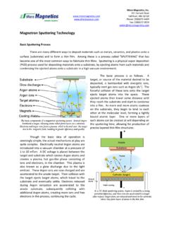
5 NanoFoil can be used to bond metals, ceramics, semiconductors and certain polymers. The bonding process allows freedom in the choice of solders and is flux-free, eliminating a cleaning operation. Sputtering used to produce foil RNT produces NanoFoil by alternately Sputtering or depositing nickel and aluminum atom by atom onto a substrate. The Sputtering process takes place in a vacuum chamber that contains the target consisting of the Material to be deposited as well as the substrate. Argon is introduced into the chamber and ionized. A Magnetron utilizes strong magnetic fields to trap electrons close to the surface of the target.
6 The positively charged argon ions accelerate towards the target and strike it with sufficient force to remove Material . The sputtered ions ballistically fly from the target and impact energetically on the substrate. After the foil has been built up onto the substrate, it is peeled off to produce the final product. The target Material can be limited by inevitable non-uniformities in the magnetic field or poor magnetic design. Our production startup was trouble-free enabling us to focus our energies on working with customers to develop applications for NanoFoil , Zimone said.
7 But RNT soon determined that they needed to reduce the costs of manufacturing the foil in order to be profitable at pricing levels that would keep the new technology competitive with alternative bonding methods. The most obvious potential area for cost-reduction was improving the utilization of the nickel target. The utilization of this target is important because the nickel target costs much more than the aluminum target and the cost of the nickel target per unit of nickel is several times the scrap value that can be obtained from the depleted target. I worked with Angstrom Sciences magnetrons while I was at several different companies and have a great deal of confidence in Angstrom s ability to design custom magnetrons to meet special requirements, Zimone said.
8 We shipped the Magnetron that we used on our development tool to Angstrom Sciences and asked them if they could improve its utilization . It was also important to ensure that the any changes made to the Magnetron did not affect the high levels of quality that we were achieving with the original Magnetron . Simulation used to improve target utilization The critical factor affecting the utilization of the target in a Magnetron is the distribution of the magnetic field used to trap electrons above the target, said Richard Newcomb, Research and Development Manager for Angstrom Sciences.
9 The region and depth of the target erosion generally mirrors the shape of the magnetic field lines one half to one inch about the surface of the target. This is because the electrons that create the discharge are accelerated around the target at approximately 90 degree angle relative to the magnetic field lines. By tuning the intensity and shape of the magnetic field, the electrons can be allowed to travel in a broad path which will ultimately lead to utilizing more of the available target surface and better uniform of thin film coatings. Figure 2: Electromagnetic simulation of existing Magnetron and new Magnetron designs shows that field lines just above target are considerably flatter with the new design Newcomb used electromagnetic simulation in an effort to optimize the magnetic fields around the target in order to improve its utilization .
10 Simulation is attractive because it enables engineers to determine the performance of a design before it is built. Engineers can quickly try out different designs in their attempt to achieve effective containment while minimizing costs. Newcomb defined the geometry of the original Magnetron , entered materials properties for the components and defined the currents and conductivities. A major advantage of electromagnetic simulation is that Newcomb was able to view the direction and magnitude of electromagnetic fields throughout the area of interest around the target.