Search results with tag "Sputtering"
Ion Beam Sputtering: Practical Applications to Electron ...
www.southbaytech.comTable 1: Description of some common target materials and their applications to electron microscopy. Biological Applications As discussed, ion beam sputtering offers many unique features for an array of EM applications. For biological materials, the use of the Model IBS/e is particularly useful due to the nature of the ion beam sputtering process.

Magnetron sputtering - University of Pennsylvania
www.seas.upenn.eduAs the accelerated electrons soon lose their ener- gy in ionising collisions most the applied voltage in a sputtering system appears across the cathode dark space. If the anode is moved closer to the 4 Figure 1. Schematic diagram of ixdiode sputtering process chamber. Figure 2. Typical variation of mean free path with pressure. Pressure (Pal

SEM sample preparation - IJS
cemm.ijs.siSPUTTERING Instead of using heat to eject material from a source, we can bombard them with high speed particles. The sputtering gas bombards the target and sputters off the material we would like to deposit. Once ejected, these atoms (or molecules) can travel to a substrate and deposit as a film.
DEPOSITED INDIUM TIN OXIDE (ITO) THIN FILMS BY DC ...
www.nipne.ro2 Deposited indium tin oxide (ITO) thin films by dc-magnetron sputtering 731 ITO films on plastic substrates by sputtering has been reported [9, 10].

Bottom up Synthesis of Nanomaterials
www.lscollege.ac.in• Sputtering Bottom-Up approach Sputter deposition are methods of depositing thin films by sputtering. They involve ejecting material from a “target” that is a source onto a “substrate” such as a silicon wafer. Sputtered atoms ejected from the target have a wide energy distribution, typically up to tens of eV. RF or DC signal
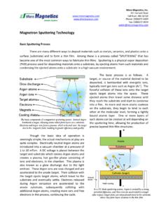
Magnetron Sputtering Technology - DirectVacuum.com
www.directvacuum.comThere are a number of ways to enhance this process. One common way to do this is to use what is known as a magnetron sputtering system.

New Magnetron Improves Sputtering Material …
www.angstromsciences.comNew Magnetron Design Improves Sputtering Material Utilization from 14% to 40% Reactive NanoTechnologies, Inc.’s (RNT) NanoFoil® foil precisely controls

Surface Engineering and Coatings
www.uobabylon.edu.iqIon Beam Sputtering A physical vapor deposition process in which the coating material (target) is removed from the surface of the coating source (cathode) by a flux of high energy ions and deposited upon the surface of substrates. It can also be used to sputter-off or clean substrate surface Dual-ion-beam sputtering
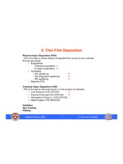
II. Thin Film Deposition - Harvard University
www.mrsec.harvard.eduRF (Radio Frequency) Sputtering DC sputtering cannot be used for depositing dielectrics because insulating cathode will cause charge build up during Ar+ bombarding ¨reduce the voltage between electrodes ¨discharge distinguishes Substrate 13.56 MHz e-Ar e-Ar+ t Target Target Sheath Substrate Sheath ~ Solution: use AC power

Filters Fluorescence and Life Science Instrumentation
www.horiba.comelement heating, Ion assisted e-Beam, and Dual Magnetron Reactive Ion Beam Sputtering; the world’s most advanced sputtering technology. No single technology is ideal for every application. as a world-class manufacturer, omega optical

The Development of Functional Thin Films and Sputtering ...
www.kobelco.co.jpKOBELCO TECHNOLOGY REVIEW NO. 26 DEC. 2005 98 The Development of Functional Thin Films and Sputtering Target Materials for Electronic Devices Dr. Junichi NAKAI, Electronics Research Laboratory, Technical Development Group

Horiba 2470 GD Profiler revision V4.qxd 2/27/06 9:29 PM Page 1
www.horiba.com6 7 Depth profile analysis is a continuous process of sputtering through a sample at a rate of typically 3 microns per minute. At such a speed, two parameters are critical.

Nanostructured Ti thin films by combining GLAD and ...
www.ispc-conference.org22nd International Symposium on Plasma Chemistry July 5-10, 2015; Antwerp, Belgium O-18-3 1 Nanostructured Ti thin films by combining GLAD and magnetron sputtering: a joint experimental and modeling …
CHAPTER 10 AUGER ELECTRON SPECTROSCOPY
www.wellesley.eduWhen a beam of electrons, typically with an energy range of 3 20 keV, strikes a solid atom, a core-level ... Auger depth profiling with noble gas ion sputtering was alkali atoms into doublets, is due to spin-orbit coupling, the interaction of the spin magnetic moment with the magnetic field arising from the orbital angular momentum.

Chapter 1 Introduction to Chemical Vapor Deposition (CVD)
www.asminternational.orgtechniques, such as sputtering or evaporation, generally require a line-of-sight between the surface to be coated and the source. Another advantage of CVD is that, in addition to the wide variety of materials that can be deposited, they can be deposited with very high purity. This results from the relative ease with which
Cu Nanoparticle: Synthesis, Characterization and Application
www.chemmethod.combeam irradiation. Among these methods, the chemical reduction method is superior because it is ... sputtering etc. Among these methods, a most noticeable method is a wet chemical synthesis; nevertheless, a more modern method is available for selectivity and control the size. ... nanoparticles in an aqueous medium at a high cupric ion ...

AN900 APPLICATION NOTE - STMicroelectronics
www.st.comelectron beam. Metal Deposition It allows the realization of electrical connections between the different cells of the integrated circuit and the outside. Two different methods are used to deposit the metal: evaporation or sputtering. "Front-End" "Back-End" WAFER FABRICATION ASSEMBLY Wafer Final Probing Test VR02103A 2

Atomic Layer Deposition - ALD Academy
www.aldacademy.cominduced evaporation or sputtering by energetic ion bom-bardment. The method of CVD, on the other hand, in-volves chemical reactions. These chemical reactions take place by volatile precursor molecules that decompose at the surface leaving a thin film and volatile by-products. The chemical reactions are thermally driven, most fre-

Optical Filters Construction of Optical Filters
www.semrock.comIon-assisted ion-beam sputtering (IBS) • Originally developed for coating precise ferrite thin films on magnetic disk drives and extremely low -loss mirrors for ring -laser gyro applications • Then adapted for extremely high-performance optical filters for Telecom/WDM in the late 1990’s • Based on hard refractory oxide materials like ...

CHAPTER 6: Etching - City University of Hong Kong
www.cityu.edu.hkexcited electronic states that later decay by photoemission, thereby causing the ... the target surface and under the operating pressure, argon ions arrive ... sputtering rates for different materials. Figure 6.6(b) depicts the schematic of a parallel - plate plasma etching system.

Nanoparticle Characterization and Application: An Overview
www.ijcmas.comchemical methods are ion sputtering, solvothermal synthesis, and sol gel technique. Basically there are two approaches for nanoparticle synthesis namely the Bottom up approach and the Top ... beam is a technique that used for removing materials from a solid surface. Absorbed

9th International Conference on HIPIMS, 27-18 June …
www.hipimsconference.com9th International Conference on HIPIMS, 27-18 June 2018, Sheffield, UK PRELIMINARY PROGRAM 5 17:20 - 17:40 Bipolar High Power Impulse Magnetron Sputtering: A …

Sputtering - Wake Forest University
users.wfu.edureduced density, electric field strength becomes weak •Electrons have the right energy to cause ... the pressure can not be too low. – The mean free path should be a tenth or less than the typical ... • The key principle is energy and momentum conservation. • In any collision, momentum is conserved. ...
Similar queries
Ion Beam Sputtering: Practical Applications to Electron, Applications to electron, Applications, Ion Beam Sputtering, Magnetron Sputtering, Ener- gy, Preparation, Sputtering, Indium tin oxide, Magnetron Sputtering Technology, New Magnetron Improves Sputtering Material, Magnetron, Improves Sputtering Material Utilization from, Beam sputtering, Thin, Sputtering Target Materials for Electronic Devices, Combining GLAD and magnetron sputtering, Modeling, CHAPTER 10 AUGER ELECTRON SPECTROSCOPY, Beam, Introduction to Chemical Vapor Deposition, Cu Nanoparticle, Optical Filters Construction of Optical Filters, Electronic, Target, Materials, Ion sputtering, Reduced, Pressure, Principle