Transcription of OB6563CP Data Sheet - DALINCOM
1 OB6563. High Performance PFC Controller DESCRIPTIONS OB6563 is offered in SOP-8 and DIP-8 packages. OB6563 is an active transition-mode (TM) power factor correction (PFC) controller for AC-DC switching mode FEATURES. power supply applications. Transition Mode (TM) Operation OB6563 features an internal start-up timer for stand- One quadrant multiplier with THD optimizer alone applications, a one quadrant multiplier with THD Low Dynamic OVP Sensing Current Setting optimizer for near unity power factor, zero current Low Start-up Current and Operating Current detector (ZCD)
2 To ensure TM operation, a current Cycle-by-Cycle Current Limiting sensing comparator with built-in leading-edge blanking, Internal RC Filter and a totem pole output ideally suited for driving a Trimmed Internal Bandgap Reference power MOSFET. Under Voltage Lockout with Hysteresis OB6563 offers great protection coverage including Dynamic and Static Output Over-Voltage Protection system over-voltage protection (OVP) to eliminate (OVP). runaway output voltage due to load removal, VCC under voltage lockout (UVLO), cycle-by-cycle current limiting, Internal Start-up Timer for Stand-alone Applications multiplier output clamping that limit maximum peak Disable Function switch current, and gate drive output clamping for Totem Pole Output with High State Clamping external power MOSFET protection.
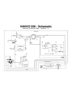
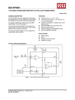
3 System Open Loop Protection With added system open loop protection feature, Proprietary Audio Noise Free Operation OB6563 shuts down system when the feedback loop is to 28V wide range of VCC voltage open. In OB6563, the dynamic OVP sensing current is set to APPLICATIONS. 10uA, which will decrease system standby power greatly. Electronic Ballast When used with On-Bright PWM controller OB2298 or AC-DC SMPS. Quasi-Resonant controller OB2203 in a 150W AC/DC. power design, it can deliver < standby power at universal AC range input. TYPICAL APPLICATION. L1 C6 R6. D2 D3.
4 C1 D1. R8 R2. R7 OB6563. C2. 1 INV VCC 8. +. AC C4 R4. Q1. 2 COMP GD 7 +. C5. 3 MULT GND 6 R5. C3. R1 4 CS ZCD 5 R3. On-Bright Electronics Confidential OB_DOC_DS_6500. -1 . OB6563. High Performance PFC Controller GENERAL INFORMATION. Terminal Assignment Package Dissipation Rating In SOP8 or DIP8 Package. Package R JA ( C/W). DIP8 90. SOP8 150. Absolute Maximum Ratings INV 1 8 VCC Symbol Parameter Value VCC DC Supply voltage 30 V. Zero Current 50mA(source). COMP 7 I_ZCD Detector Max. 2 GD -10mA(sink). Current CS. INV Analog inputs &. COMP. to 7V. 6 outputs MULT 3 GND MULT.
5 Min/Max Operating Tj Junction -20 to 150 oC. 5 Temperature CS 4 ZCD. Min/Max Storage Tstg -55 to 150 oC. Temperature Lead (Soldering, 10secs) 260 oC. Temperature Ordering Information Note: Stresses beyond those listed under absolute maximum Part Number Description ratings may cause permanent damage to the device. These are OB6563AP 8 Pin DIP, Pb free in Tube stress ratings only, functional operation of the device at these OB6563CP 8 Pin SOP, Pb free in Tube or any other conditions beyond those indicated under OB6563 CPA 8 Pin SOP, Pb free in T&R recommended operating conditions is not implied.
6 Exposure to absolute maximum-rated conditions for extended periods may affect device reliability. On-Bright Electronics Confidential OB_DOC_DS_6500. -2 . OB6563. High Performance PFC Controller Marking Information TERMINAL DESCRIPTIONS. Pin Num Pin Name I/O Description 1 INV I Inverting Input of Error Amplifier. Connected to Resistor Divider from System Output. This pin is also used for system open loop protection. 2 COMP O Output of Error Amplifier. A feedback compensation network is placed between COMP and the INV pin. 3 MULT I Input of Multiplier. Connected to Line Voltage after Bridge Diodes via A.
7 Resistor Divider to Provide Sinusoidal Reference Voltage to the Current Loop. 4 CS I Current Sense Input Pin. Connected to MOSFET Current Sensing Node. 5 ZCD I Zero Current Detection Input. When Activated, A New Switching Cycle Starts. If it is connected to GND, the device is disabled. 6 GND P Ground Pin 7 GD O Gate driver output. Drive Power MOSFET. 8 VCC P DC Supply Voltage. On-Bright Electronics Confidential OB_DOC_DS_6500. -3 . OB6563. High Performance PFC Controller BLOCK DIAGRAM. On-Bright Electronics Confidential OB_DOC_DS_6500. -4- OB6563. High Performance PFC Controller ELECTRICAL CHARACTERISTICS.
8 (TA = 25OC if not otherwise noted). Symbol Pin Parameter Test Conditions Min Typ Max Unit SUPPLY VOLTAGE SECTION. Vcc 8 Operating Range After Turn On 11 28 V. 8 Turn-on Threshold 11 12 13 V. UVLO. 8 Turn-off Threshold V. Hys 8 Hysteresis V. Vz 8 Zener Voltage Icc=5mA 30 33 36 V. SUPPLY CURRENT SECTION. Icc-start 8 Start-up Current Vcc=11V 35 70 uA. Iq 8 Quiescent Current, No Vcc= 4 mA. Switching Icc 8 Operating Supply Current CL=1nf @ 70kHz 4 mA. In OVP condition mA. Vpin1= Iq 8 Quiescent Current Vpin5 150mV mA. Vcc= Vpin5 150mV, Vcc<Vcc 35 70 uA. off ERROR AMPLIFIER SECTION.
9 Voltage Feedback Input Vinv 1 Vcc= V. Threshold Vinv 1 Line Regulation 12V<Vcc<28V 2 5 mV. Iinv 1 Input Bias Current IDD = 10 mA -1 uA. Gv Voltage Gain Open Loop 60 80 dB. Gb Gain Bandwidth MHz Source Current Vcomp= , Vinv= -1 -3 -5 mA. Icomp 2. Sink Current Vcomp= , Vinv= 1 3 5 mA. Upper Clamp Voltage Isource= V. Vcomp 2. Lower Clamp Voltage Isink= V. MULTIPLIER SECTION. Vmult 3 Linear Operating Range Vcomp= 0 to V. Vcs/ Output Max. Slope Vmult=from 0 to V/V. Vmult Vcomp=Upper Clamp Voltage K Gain Vmult=1V, Vcomp= 1/V. CURRENT SENSE COMPARATOR. Vcs 4 Current Sense Reference Vmult= V.
10 Clamp Vcomp=Upper Clamp Voltage Ics 4 Input Bias Current Vcs=0 uA. Td(H-L) 4 Delay to Output 200 450 ns On-Bright Electronics Confidential OB_DOC_DS_6500. -5- OB6563. High Performance PFC Controller ELECTRICAL CHARACTERISTICS (Continued). (TA = 25OC if not otherwise noted). Symbol Pin Parameter Test Conditions Min Typ Max Unit ZERO CURRENT DETECTOR. Vzcd 5 Input Threshold Voltage V. Rising Edge Hysteresis V. Vzcd 5 Upper Clamp Voltage Izcd= V. Vzcd 5 Lower Clamp Voltage Izcd= V. Izcd 5 Input Bias Current 1V Vzcd 2 uA. Izcd 5 Source Current Capability -3 -5 mA.