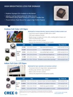
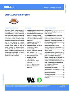
Transcription of Optimizing PCB Thermal Performance for Cree …
1 Product design guideCopyright 2010-2018 Cree, Inc. All rights reserved. The information in this document is subject to change without notice. Cree and XLamp are registered trademarks and the Cree logo is a trademark of Cree, Inc. This document is provided for informational purposes only and is not a warranty or a specification. For product specifications, please see the data sheets available at For warranty information, please contact Cree Sales at Cree, Silicon DriveDurham, NC 27703 USA Tel: + Rev 2 JOptimizing PCB Thermal Performance for Cree XLamp LEDsInTrODuCTIOnThis Cree application note outlines a technique to assist with the development of cost-effective Thermal management for the XT, XP, XB, MX and ML families of XLamp of the most critical design parameters for an LeD illumination system is the system s ability to draw heat away from the LeD junction.
2 High operating temperatures at the LeD junction adversely affect the Performance of LeDs, resulting in decreased light output and To properly manage this heat, specific practices should be followed in the design, assembly and operation of LeDs in lighting application note outlines a technique for designing a low-cost printed circuit board (PCB) layout that optimizes the transfer of heat from the LeD. The technique involves the use of FR-4-based PCBs, which cost less than metal core printed circuit boards (MCPCB), but have greater Thermal resistance. The use of metal-lined holes or vias underneath LeD Thermal pads is a method to dissipate heat through an FR-4 PCB and into an appropriate heat XLamp LeDs are designed with an electrically isolated Thermal path.
3 Cree pioneered this LeD feature almost ten years ago to enable the use of 1 See the Long-Term Lumen Maintenance application vias in FR-4 PCBs. For certain illumination systems design, Thermal vias enable the use of FR-4 circuit boards instead of metal core circuit boards. This can deliver system cost savings in circuit board and heat sink application note serves as a practical guideline based on heat transfer fundamentals and includes suggestive, but not definitive, simulation and measurement data. Cree advocates this technique as appropriate design for certain lighting applications and encourages Cree s customers to evaluate this option when considering the many Thermal management techniques available. For additional guidelines on LeD Thermal management, refer to the Thermal Management application O f COnTEnTsIntroduction.
4 1 Thermal Management Principles ..2 XLamp LeD Thermal Characteristics ..2 PCB Thermal Characteristics ..3 Designing Thermal vias ..4 Open vias vs. Filled vias ..5 Thermal Performance Simulations ..7 Surface Thermal Dissipation ..7 Thermal Dissipation with vias ..8 Combined Surface and via Studies 10 Summary Results of Thermal Simulations ..12 Temperature Verification Measurements ..13 Recommended Board Layouts ..15 Gerber files ..15FR-4 Boards for XLamp XP and XT LeD Packages ..16FR-4 Boards for XLamp XB LeD Package ..17FR-4 Boards for XLamp MX LeD Package ..19FR-4 Boards for XLamp ML LeD Package ..20 Chemical ..21 Copyright 2010-2018 Cree, Inc. All rights reserved. The information in this document is subject to change without notice. Cree and XLamp are registered trademarks and the Cree logo is a trademark of Cree, Inc. This document is provided for informational purposes only and is not a warranty or a specification.
5 For product specifications, please see the data sheets available at For warranty information, please contact Cree Sales at PCB Thermal PeRFORMANCeThErmaL managEmEnT PrInCIPLEsThe technique in this application note is not recommended for Cree LEDs that consume more than 5 W of power, including MC-E and MT-G2. For low-power applications, this technique can be used for XM-L LED Thermal CharacteristicsAll XLamp LeD packages have an electrically isolated Thermal pad. The pad provides an effective channel for heat transfer and optimizes Thermal resistance from the LeD chip junction to the Thermal pad. The pad is electrically isolated from the anode and cathode of the LeD and can be soldered or attached directly to grounded elements on the board or heat sink 1: Cree XLamp XP LED packageHeat is conducted from the LeD package through the Thermal pad and into a PCB that should be mounted to a heat sink to transfer the conducted heat into the operating 1 and 2 list typical Thermal resistance values (junction to solder point) for various XLamp series 1: Typical Thermal resistance values for Cree XLamp white LEDsColorThermal resistance ( C/W)mL-BmL-CmL-Em X- 3m X- 6XB-DXm-LXm-L EZWXP-CXP-EXP-gXT-EWhite (cool, neutral, warm) 2.
6 Typical Thermal resistance values for Cree XLamp color LEDs n/a indicates an LED that Cree does not offerColorThermal resistance ( C/W)mL-EXP-CXP-ERoyal bluen/a129 Blue11129 Green152015 Ambern/a1510 Red151010 Red-orangen/a10102 For subsequent discussion and simulation in this document, we assume the PCB is mounted to an infinite heat sink that maintains the back side of the board at 25 1. Cree XLamp XP LED PackageLED LensAnode CathodeAl NsubstrateLED chipThermal padCeramic substrateCopyright 2010-2018 Cree, Inc. All rights reserved. The information in this document is subject to change without notice. Cree and XLamp are registered trademarks and the Cree logo is a trademark of Cree, Inc. This document is provided for informational purposes only and is not a warranty or a specification. For product specifications, please see the data sheets available at For warranty information, please contact Cree Sales at PCB Thermal PeRFORMANCePCB Thermal Characteristicsfr-4FR-4 is one of the most commonly used PCB materials and is the National electrical Manufacturers Association (NeMA) designation for a flame retardant, fiberglass-reinforced epoxy laminate.
7 A by-product of this construction is that FR-4 has very low Thermal conductivity. Figure 2 below shows a typical cross-sectional geometry for a two-layer FR-4 2: fr-4 cross-sectional geometry (not to scale)Using the Thermal conductivity values in Table 3 below, the total Thermal resistance for an FR-4 board can be calculated by adding the Thermal resistances of the layers. PCB = layer1 + layer2 + layer3 .. + layerN (1)For a given layer the Thermal resistance is given by the formula: = l / (k x A) (2)where l is the layer thickness, k is the Thermal conductivity, and A is the area normal to the heat a thick star board approximately 270 mm2, the calculated through-plane Thermal resistance is approximately 30 C/W. Bear in mind that this calculation is one-dimensional and does not account for the size of the heat source, spreading, convection Thermal resistances or boundary conditions.
8 If a smaller heat source size is considered, for example mm x mm, the resulting one-dimensional Thermal resistance increases to over 700 3: Typical Thermal conductivities of fr-4 board layersLayer/materialThickness ( m) Thermal conductivity (W/mK)SnAgCu solder7558 Top layer copper70398FR-4 layer copper70398electroless Nickel/Immersion Gold (eNIG) Printed Circuit BoardA simple one-layer MCPCB is comprised of a solder mask, copper circuit layer, thermally conductive dielectric layer, and metal core base layer, as shown below in Figure 3. These three layers are laminated and bonded together, providing a path for the heat to dissipate. Often the metal substrate is aluminum, though steel and copper can also be 2: FR-4 cross -sectional geometry (not to scale) Solder mask Bottom layer Cu FR4 dielectric Top layer Cu Thermal pad Heat source ENIG Copyright 2010-2018 Cree, Inc.
9 All rights reserved. The information in this document is subject to change without notice. Cree and XLamp are registered trademarks and the Cree logo is a trademark of Cree, Inc. This document is provided for informational purposes only and is not a warranty or a specification. For product specifications, please see the data sheets available at For warranty information, please contact Cree Sales at PCB Thermal PeRFORMANC efigure 3: mCPCB cross-sectional geometry (not to scale)Using the Thermal conductivity values in Table 4 below, the one-dimensional through-plane Thermal resistance for a star board of approximately 270 mm2 is roughly C/W. If a smaller heat source size is considered, the resulting Thermal resistance is C/W. In this case, the limiting factor is the PCB 4: Typical Thermal conductivities of mCPCB layersLayer/materialThickness ( m) Thermal conductivity (W/mK)SnAgCu solder7558 Top layer copper70398 PCB plate1588150 Designing Thermal ViasAn inexpensive way to improve Thermal transfer for FR-4 PCBs is to add Thermal vias - plated through-holes (PTH) between conductive layers.
10 Vias are created by drilling holes and copper plating them, in the same way that a PTH or via is used for electrical interconnections between 4: fr-4 cross-sectional geometry with Thermal vias (not to scale)Figure 3: MCPCB cross-sectional geometry (not to scale) Solder mask Dielectric layer Top layer Cu Thermal pad Heat source Al substrate Copyright 2010-2018 Cree, Inc. All rights reserved. The information in this document is subject to change without notice. Cree and XLamp are registered trademarks and the Cree logo is a trademark of Cree, Inc. This document is provided for informational purposes only and is not a warranty or a specification. For product specifications, please see the data sheets available at For warranty information, please contact Cree Sales at PCB Thermal PeRFORMANC efigure 5: Cross-sectional geometry of small and large Thermal vias in fr-4 substrateAdding vias in an appropriate way will improve the Thermal resistance of an FR-4 board.