Transcription of Pierce-Gate Crystal Oscillator, an introduction
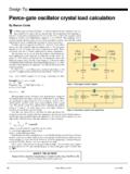
1 PAGE MARCH 2008 ARTICLE IntroductionThe most common gate oscillator in use today is by far the Pierce-Gate shown in Figure 1. Its popular-ity stems from the fact that the digital inverter, U1, is usually included in the microprocessor or ASIC the designer selects. In effect, the oscillator cell U1 is free!Most designers are familiar with the Pierce-Gate topology, but few really understand how it functions, let alone how to properly design it. As a common practice, most don t even pay too much attention to the oscil-lator in their design until it does not func-tion properly, usually already released to production. This should not be case. Many systems or projects have been delayed in their deployment because of a twenty-five cent Crystal not working as intended.
2 The oscillator should receive its proper amount of attention during the design phase, well before the manufacturing phase. The designer would then avoid the nightmare scenario of product being returned from the will analyze how the Pierce-Gate oscillator functions by breaking it down to its components. (A much more rigorous analysis is beyond the scope of this paper.) However, the simple analysis will suffice to convey the key points of Pierce-Gate Oscillator operation. In addition, we ll pres-ent a simple design problem to teach how to derive at the Pierce-Gate initial Basic Pierce-Gate OscillatorWe can use the Barkhausen criteria to explain how the Pierce-Gate topology works. The criteria states the following:The product of the gains around the loop must be equal to or greater than one at the desired frequency of phase shift around the loop must be zero or any integer multiple of 2 (360 ).
3 Figure 2 shows the phase shift analysis for the Pierce-Gate . If U1 provides -180 phase shift, an additional -180 by the rest of external components is required to sat-isfy the Barkhausen criteria. The phase shift will automatically adjust itself to be exactly 360 around the loop in order to keep oscil-lating. If U1 provides -185 phase shift, the rest of the components will automati-cally provide -175 phase shift in a properly gain around the loop is a func-tion of gm (transconductance) of the inverter and reactance of C1 and C2 (Xc1, Xc2) and Rs. Without Rs in the loop, the gain in terms of negative resistance is: 12negative resistance=CCgmXX Eq. 1 Since 1/CXjwc=, the negative resis-tance (gain) goes up as the capacitors C1 and C2 are reduced.
4 Hence, decrease C1 and C2 to increase the gain around the loop. It is easy to see that Rs decreases the gain around the loop as its value is increased. A starting value for Rs is to set it equal to the reactance of Resistor RfThe feedback resistor Rf is there to linearize the digital CMOS inverter. Rf accomplishes this feat by charging the inverter s input capacitance, including C1 from the output of the inverter. In other words, the feedback resistor transforms a logic gate into an ana-log amplifier. Pretty neat trick by simply adding a single the feedback resistor is includ-ed with the micro or ASIC. Use the follow-ing procedure to determine if the feedback resistor is integrated in the IC:With no external components connected (C1, C2 and X1), measure the voltage at the input and output of the the feedback resistor is inside, then the voltage at the input and output pins will be around Vcc/2.
5 If the feedback resistor in not inside, then the inverter will be latched and either the input and output will be at a logic 1 or logic 0 or vice-versa. The value of Rf used is frequency-depen-dent. The lower the frequency, the higher the value needed. Table 1 lists typical range feedback resistance Rf can be opti-mized in the following manner:With the Crystal and all other compo-nents in place, determine the value of Rf which begins to pull the frequency. Do this by plotting frequency vs. Rf. Choose the value of Rf above the point where loading begins to pull the RsThe resistor in series with the output of the inverter, Rs, has three primary functions:To isolate the output driver of the inverter from the complex impedance formed by C2, C1 and the give the designer another degree of freedom to control the drive level (expressed as power/voltage across or Crystal Oscillator, an introductionby Ramon Cerda, Director of Engineering, Crystek CorporationFigure 1: Fundamental Mode Isolated Pierce- gate OscillatorFigure 2: Pierce-Gate Phase Shift AnalysisTable 1.)
6 Typical range values for feedback resistor RfFrequencyFeedback Resistor KHz10~15 Meg ohms1 MHz5~10 Meg ohms10 MHz1~5 Meg ohms20 MHz470 K to 5 Meg ohmsPAGE 2 MARCH 2008 ARTICLE current through the Crystal ) and/or adjust the oscillator loop gain. Rs must be used with Tuning-Fork (watch) crystals. Tuning-Fork crystals have a maximum drive level of 1 W maximum. Without a large Rs (greater than 10k ohms), the inverter will physically damage the Crystal ! In conjunction with C2, Rs forms a lag network to add additional phase shift necessary especially at low frequen-cies, 8 MHz or below. This additional phase shift is needed to reduce the jit-ter in the time domain or phase noise in frequency domain. Rs is sometimes not needed (especially at frequencies above 20 MHz) since the output resis-tance of the inverter in conjunction with C2 will provide enough phase lag.
7 However, when not be needed to phase lag it may still be needed to reduce the drive level on the U1 The inverter U1 provides the necessary loop gain to sustain oscillation as well as approximately -180 phase shift. If the inverter is part of some ASIC or micropro-cessor, its manufacturer should specify the critical Crystal parameters like maximum that will work properly under all conditions. If U1 is not part an ASIC, then the designer must carefully select an inverter with the proper gain/phase charac-teristics for the targeted frequency or range of frequencies. Simulation is also strongly recommended here but not necessary for a good working design. Not all digital invert-ers are suitable for oscillator applications.
8 Some have too much propagation delay, even at low frequencies. On the other hand, in the past one needed an inverter with no buffer (un-buffered) for oscillators . This is not the case today since propagation delays have been reduced over the years for all modern digital inverters due to the required higher speeds of call to the inverter manufacturer s technical support department is a good idea to get their blessing (in a sense) of your intended use as an X1, Capacitors C1 and C2As mentioned above, the Crystal X1, together with C1, C2 and Rs, provide an additional -180 phase lag to satisfy the Barkhausen phase shift criteria for sustain-ing oscillation. In most cases C1 is set equal to C2. However, if need be, C2 can be made larger than C1 by a few standard values and set the center frequency and/or increase the loop gain.
9 There is step-up in voltage gain that is function C2 Crystal X1 in Figure 1 needs to be Parallel Mode , Fundamental crys-tal. In the Pierce-Gate oscillator, the Crystal works in the inductive region of its reac-tance curve. A Crystal that needs to operate in its inductive region is called a Parallel Crystal . Pierce-Gate Design ExampleDesign a 20 MHz CLOCK using the Pierce-Gate topology given the following require-ments:Frequency: 20 MHzFrequency vs. temperature stability: +/-50 ppmCalibration/tolerance at +25C: +/-50 ppmTemperature range: -20 to +70 CAdditional requirements are:low costAll SMT componentsNo factory adjustment of components to meet the +/-50 ppm calibration are:The inverter gate is part of a micropro-cessor with Cin = 4 pF and Cout = 9 pF.
10 The feedback resistor Rs is not internal as shown in Figure 1. The microprocessor manufacturer has already determined that a Crystal with an = 40 ohms maximum will provide reliable operation at this : C1, C2, Rs, Rf, and specify the , let us choose a value for Rf. This component is not critical for this design and can be within 470k~5 Meg ohms at this frequency as listed in Table 1. Therefore choose Rf = 1 Meg ohm. The value of C1 and C2 together with Cin and Cout of the inverter (see Fig. 3) will set the load capacitance requirement on the Crystal . For a clock design, you want to have the load capacitance specification of the Crystal to be about the standard values of 18 or 20 pF.