Transcription of Programmable Serial Channel 8-bit Microcontroller - Keil
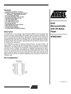
1 1 (RXD) (TXD) (INT0) (INT1) (T0) (T1) (AD4) (AD5) (AD6) (AD7)EA/ (A15) (A14) (A13)44434241403938373635341213141516171 819202122(WR) (RD) (A8) (A9) (A10) (A11) (A12) (T2 EX) (T2) (AD0) (AD1) (AD2) (AD3)Features Compatible with MCS-51 Products 4K Bytes of In-System Reprogrammable Flash Memory Endurance: 1,000 Write/Erase Cycles Fully Static Operation: 0 Hz to 24 MHz Three-level Program Memory Lock 128 x 8-bit Internal RAM 32 Programmable I/O Lines Two 16-bit Timer/Counters Six Interrupt Sources Programmable Serial Channel Low-power Idle and Power-down ModesDescriptionThe at89c51 is a low-power, high-performance CMOS 8-bit microcomputer with 4 Kbytes of Flash Programmable and erasable read only memory (PEROM). The deviceis manufactured using Atmel s high-density nonvolatile memory technology and iscompatible with the industry-standard MCS-51 instruction set and pinout.
2 The on-chipFlash allows the program memory to be reprogrammed in-system or by a conven-tional nonvolatile memory programmer. By combining a versatile 8-bit CPU with Flashon a monolithic chip, the Atmel at89c51 is a powerful microcomputer which providesa highly-flexible and cost-effective solution to many embedded control (RXD) (TXD) (INT0) (INT1) (T0) (T1) (WR) (RD) (AD0) (AD1) (AD2) (AD3) (AD4) (AD5) (AD6) (AD7)EA/ (A15) (A14) (A13) (A12) (A11) (A10) (A9) (A8)Rev. 0265G 02/008-bit Microcontroller with 4K Bytes FlashAT 8 9 C 5 1 Not Recommended for New Designs. Use (RXD) (TXD) (INT0) (INT1) (T0) (T1) (AD4) (AD5) (AD6) (AD7)EA/ (A15) (A14) (A13)65432144434241401819202122232425262 728(WR) (RD) (A8) (A9) (A10) (A11) (A12) (AD0) (AD1) (AD2) (AD3)AT89C512 Block DiagramPORT 2 DRIVERSPORT - 0 LATCHRAMPROGRAMADDRESSREGISTERBUFFERPCIN CREMENTERPROGRAMCOUNTERDPTRRAM , Serial PORT,AND TIMER BLOCKSSTACKPOINTERACCTMP2 TMP1 ALUPSWTIMINGANDCONTROLPORT 3 LATCHPORT 3 - 1 LATCHPORT 1 - / VPPRSTPORT 0 - at89c51 provides the following standard features: 4 Kbytes of Flash, 128 bytes of RAM, 32 I/O lines, two 16-bittimer/counters, a five vector two-level interrupt architecture,a full duplex Serial port, on-chip oscillator and clock cir-cuitry.
3 In addition, the at89c51 is designed with static logicfor operation down to zero frequency and supports twosoftware selectable power saving modes. The Idle Modestops the CPU while allowing the RAM, timer/counters, Serial port and interrupt system to continue functioning. ThePower-down Mode saves the RAM contents but freezesthe oscillator disabling all other chip functions until the nexthardware DescriptionVCCS upply 0 Port 0 is an 8-bit open-drain bi-directional I/O port. As anoutput port, each pin can sink eight TTL inputs. When 1sare written to port 0 pins, the pins can be used as high-impedance inputs. Port 0 may also be configured to be the multiplexed low-order address/data bus during accesses to external pro-gram and data memory. In this mode P0 has 0 also receives the code bytes during Flash program-ming, and outputs the code bytes during programverification.
4 External pullups are required during programverification. Port 1 Port 1 is an 8-bit bi-directional I/O port with internal Port 1 output buffers can sink/source four TTL 1s are written to Port 1 pins they are pulled high bythe internal pullups and can be used as inputs. As inputs,Port 1 pins that are externally being pulled low will sourcecurrent (IIL) because of the internal pullups. Port 1 also receives the low-order address bytes duringFlash programming and verification. Port 2 Port 2 is an 8-bit bi-directional I/O port with internal Port 2 output buffers can sink/source four TTL 1s are written to Port 2 pins they are pulled high bythe internal pullups and can be used as inputs. As inputs,Port 2 pins that are externally being pulled low will sourcecurrent (IIL) because of the internal pullups.
5 Port 2 emits the high-order address byte during fetchesfrom external program memory and during accesses toexternal data memory that use 16-bit addresses (MOVX In this application, it uses strong internal pullupswhen emitting 1s. During accesses to external data mem-ory that use 8-bit addresses (MOVX @ RI), Port 2 emits thecontents of the P2 Special Function Register. Port 2 also receives the high-order address bits and somecontrol signals during Flash programming and 3 Port 3 is an 8-bit bi-directional I/O port with internal Port 3 output buffers can sink/source four TTL 1s are written to Port 3 pins they are pulled high bythe internal pullups and can be used as inputs. As inputs,Port 3 pins that are externally being pulled low will sourcecurrent (IIL) because of the 3 also serves the functions of various special featuresof the at89c51 as listed below:Port 3 also receives some control signals for Flash pro-gramming and verification.)
6 RSTR eset input. A high on this pin for two machine cycles whilethe oscillator is running resets the device. ALE/PROGA ddress Latch Enable output pulse for latching the low byteof the address during accesses to external memory. Thispin is also the program pulse input (PROG) during Flashprogramming. In normal operation ALE is emitted at a constant rate of 1/6the oscillator frequency, and may be used for external tim-ing or clocking purposes. Note, however, that one ALEPort PinAlternate ( Serial input port) ( Serial output port) (external interrupt 0) (external interrupt 1) (timer 0 external input) (timer 1 external input) (external data memory write strobe) (external data memory read strobe)AT89C514pulse is skipped during each access to external DataMemory.
7 If desired, ALE operation can be disabled by setting bit 0 ofSFR location 8EH. With the bit set, ALE is active only dur-ing a MOVX or MOVC instruction. Otherwise, the pin isweakly pulled high. Setting the ALE-disable bit has noeffect if the Microcontroller is in external execution Store Enable is the read strobe to external pro-gram memory. When the at89c51 is executing code from external pro-gram memory, PSEN is activated twice each machinecycle, except that two PSEN activations are skipped duringeach access to external data memory. EA/VPPE xternal Access Enable. EA must be strapped to GND inorder to enable the device to fetch code from external pro-gram memory locations starting at 0000H up to , however, that if lock bit 1 is programmed, EA will beinternally latched on reset.
8 EA should be strapped to VCC for internal pin also receives the 12-volt programming enable volt-age (VPP) during Flash programming, for parts that require12-volt to the inverting oscillator amplifier and input to theinternal clock operating circuit. XTAL2 Output from the inverting oscillator Characteristics XTAL1 and XTAL2 are the input and output, respectively,of an inverting amplifier which can be configured for use asan on-chip oscillator, as shown in Figure 1. Either a quartzcrystal or ceramic resonator may be used. To drive thedevice from an external clock source, XTAL2 should be leftunconnected while XTAL1 is driven as shown in Figure are no requirements on the duty cycle of the externalclock signal, since the input to the internal clocking circuitryis through a divide-by-two flip-flop, but minimum and maxi-mum voltage high and low time specifications must Mode In idle mode, the CPU puts itself to sleep while all the on-chip peripherals remain active.
9 The mode is invoked bysoftware. The content of the on-chip RAM and all the spe-cial functions registers remain unchanged during thismode. The idle mode can be terminated by any enabledinterrupt or by a hardware reset. It should be noted that when idle is terminated by a hardware reset, the device normally resumes program execu-tion, from where it left off, up to two machine cycles beforethe internal reset algorithm takes control. On-chip hardwareinhibits access to internal RAM in this event, but access tothe port pins is not inhibited. To eliminate the possibility ofan unexpected write to a port pin when Idle is terminated byreset, the instruction following the one that invokes Idleshould not be one that writes to a port pin or to 1. Oscillator ConnectionsNote:C1, C2 = 30 pF 10 pF for Crystals= 40 pF 10 pF for Ceramic ResonatorsC2 XTAL2 GNDXTAL1C1 Status of External Pins During Idle and Power-down ModesModeProgram MemoryALEPSENPORT0 PORT1 PORT2 PORT3 IdleInternal11 DataDataDataDataIdleExternal11 FloatDataAddressDataPower-downInternal00 DataDataDataDataPower-downExternal00 FloatDataDataDataAT89C515 Figure 2.
10 External Clock Drive ConfigurationPower-down Mode In the power-down mode, the oscillator is stopped, and theinstruction that invokes power-down is the last instructionexecuted. The on-chip RAM and Special Function Regis-ters retain their values until the power-down mode isterminated. The only exit from power-down is a hardwarereset. Reset redefines the SFRs but does not change theon-chip RAM. The reset should not be activated before VCCis restored to its normal operating level and must be heldactive long enough to allow the oscillator to restart Memory Lock Bits On the chip are three lock bits which can be left unpro-grammed (U) or can be programmed (P) to obtain theadditional features listed in the table lock bit 1 is programmed, the logic level at the EA pinis sampled and latched during reset.