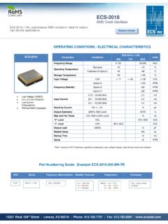
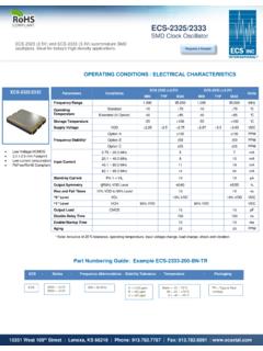
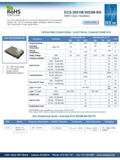
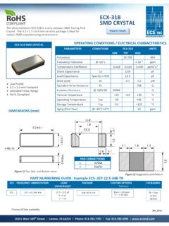
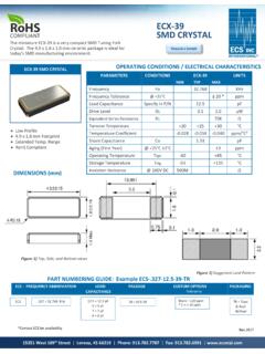
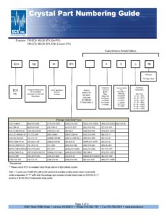
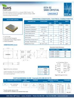
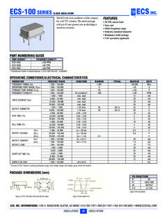
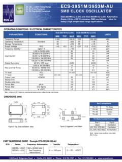
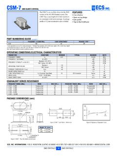
Transcription of QUARTZ CRYSTAL DESIGN PARAMETERS
1 ECS, INC. INTERNATIONAL1105 S. RIDGEVIEW, OLATHE, KS 66062 913-782-7787 800-237-1041 FAX 913-782-6991 REFERENCE TECHNICAL REFERENCE 78 QUARTZ CRYSTAL DESIGN PARAMETERSS eries vs. Parallel: Series resonant crystals are intended for use incircuits which contain no reactive components in the oscillator feedbackloop. Parallel resonant crystals are intended for use in circuits whichcontain reactive components (usually capacitors) in the oscillatorfeedback loop. Such circuits depend on the combination of the reactivecomponents and the CRYSTAL to accomplish the phase shift necessary tostart and maintain oscillation at the specified frequency. Basic depictionsof two such circuits are shown Capacitance:This refers to capacitance external to the CRYSTAL ,contained within the feedback loop of the oscillator circuit. If theapplication requires a parallel resonant CRYSTAL , the value of loadcapacitance must be specified.
2 If the application requires a series resonant CRYSTAL , load capacitance is not a factor and need not bespecified. Load capacitance is the amount of capacitance measured orcomputed across the CRYSTAL terminals on the Tolerance:Frequency tolerance refers to the allowabledeviation from nominal, in parts per million (PPM), at a specifictemperature, usually +25 Stability:Frequency stability refers to the allowabledeviation, in parts per million (PPM), over a specified temperature is referenced to the measured frequency at +25 : Aging refers to the cumulative change in frequency experiencedby a CRYSTAL unit over time. The rate of frequency change is fastest duringthe first 45 days of operation. The most common factors affecting aginginclude drive level, internal contamination, CRYSTAL surface change,ambient temperature, wire fatigue and frictional wear. All these problemscan be minimized by proper circuit DESIGN which allows for lowoperating temperatures, minimum drive levels and static : Pullability refers to the change in frequency of a crystalunit, either from the natural resonant frequency (Fr) to a load resonantfrequency (FL), or from one load resonant frequency to another.
3 SeeFigure C. The amount of pullability exhibited by a given CRYSTAL unit at agiven value of load capacitance is a function of the shunt capacitance (CO)and the motional capacitance (C1) of the CRYSTAL pullability is a factor in DESIGN , collaboration with our engineers isadvisable; bandwidth can be controlled to some extent, duringfabrication, by varying the CRYSTAL PARAMETERS . An approximation of thepulling limits for standard crystals can be obtained from the followingformula:The exact limits also depend upon the Q of the CRYSTAL as well asassociated stray capacitances. Pullability can be approximately doubledby modified CRYSTAL fabrication and by adding capacitance or inductanceexternal to the CRYSTAL . If the CO and C1 are known then the pulling inppm between two capacitances can be obtained using the = pFCL1 = 20 pFC0 = pFCL2 = 30 pFTo obtain AVERAGE pulling per pF about a known load capacitance usethe following Using figures as above and 30 pF CLEquivalent Circuit: The equivalent circuit, shown in Figure B is anelectrical depiction of the QUARTZ CRYSTAL unit when operating at afrequency of natural resonance.
4 The CO, or shunt capacitance, representsthe capacitance of the CRYSTAL electrodes plus the capacitance of the holderand leads. R1, C1, and L1compose the motional arm of the CRYSTAL andare referred to as the motional PARAMETERS . The motional inductance (L1),represents the vibrating mass of the CRYSTAL unit. The motionalcapacitance (C1), represents the elasticity of the QUARTZ and the resistance(R1), represents bulk losses occurring within the 180 ICFigure A) Depictions of Series and Parallel Resonant Circuits f= fsCO+CLC1ppm = 2(C0+ CL2)(C0+CL1)C1(CL2- CL1) 106ppm = 2( + 30) ( + 20)= (30 20)106ppm/pF = 2( + 30)2 = ppm/pF x 106ppm = 2(C0 +CL)2 C1x 106R1C1L1C0 Figure B) Equivalent CircuitECS, INC. INTERNATIONAL1105 S. RIDGEVIEW, OLATHE, KS 66062 913-782-7787 800-237-1041 FAX 913-782-6991 REFERENCE TECHNICAL REFERENCE 79 Impedance/Reactance Curve: A CRYSTAL has two frequencies of zerophase, as illustrated in Figure D.
5 The first, or lower of the two, is theSeries Resonant Frequency, denoted as ( s). At this point, the crystalappears resistive in the circuit, impedance is at a minimum and currentflow is maximum. As the frequency is increased beyond the point ofseries resonance, the CRYSTAL appears inductive in the circuit. When thereactances of the motional inductance and shunt capacitance cancel, thecrystal is at the Frequency of Anti-resonance, denoted as ( a). At thispoint, impedance is maximized and current flow is Characteristics:Although crystals are designed to handlenormal shock in handling, shock impulses (such as half sine, square,sawtooth and complex combinations) can occur in the field. Becausecrystals are relatively delicate, they should be isolated from equipment tominimize shock damage. But, avoid overspecification, since the elasticproperties of the materials and the degree of isolation afforded by theequipment can decrease the destructive potential of a Factor (Q): The Q value of a CRYSTAL unit is a measure of theunits relative quality, or efficiency of oscillation.
6 The maximum attainablestability of a CRYSTAL unit is dependent on the Q value. In Figure D theseparation between the series and parallel frequencies is called thebandwidth. The smaller the bandwidth, the higher the Q value, and thesteeper the slope of the reactance. Changes in the reactance of externalcircuit components have less effect (less pullability ) on a high Q CRYSTAL , therefore such a part is more CRYSTAL DESIGN PARAMETERS101520 253035404550 556065707580859095 100700600500400300200100 0 DELTA FREQUENCY IN PPMLOAD CAPACITANCE IN PICO FARADS (pF)DELTA FREQUENCY vs LOAD CAPACITANCES hape of curve will be constant regardless of values or overtones(Values are for reference only)Figure C) Pullability CurveREACTANCEIMPEDANCEANTI-RESONANCEfLA REA OFUSUALPARALLELRESONANCEfsSERIESRESONANC E 0+ffffa1 CoWFigure D) Reactance vs. Frequency CurveECS, INC. INTERNATIONAL1105 S. RIDGEVIEW, OLATHE, KS 66062 913-782-7787 800-237-1041 FAX 913-782-6991 REFERENCE TECHNICAL REFERENCE 80 Calculation of Load Capacitance: If the circuit configuration is asshown in Figure A for the parallel version, the load capacitance may becalculated by means of the following equation:C stray includes the pin to pin input and output capacitance of themicroprocessor chip at the CRYSTAL 1and CRYSTAL 2pins, plus any parasiticcapacitances.
7 As a rule of thumb, Cstray may be assumed to equal , if CL1= CL2= 5 OpF, CL = Sensitivity: Trim sensitivity is a measure of the incrementalfractional frequency change for an incremental change in the value of theload capacitance. Trim sensitivity (S) is expressed in terms of PPM/pFand is calculated by the following equation:Where (Ct) is the sum of Co and Reflow of Surface Mount Devices: Mounting of SMDunits is typically accomplished by means of solder reflow, as indicated inFigure E either by infrared heat or by vapor phase. The following graphsdepicts the recommended times and temperatures for each of the twomethods:Soldering Characteristics:A variety ot methods can be used tosolder ECS products to and substrates: Wave or Dual Wave Hot Air or Convection Flow Vapor Phase Reflow Infrared Reflow Bubble Solder Immersion Other (Laser, etc.)Due to the natural characteristics of material, some of our productscannot withstand heat shock.
8 Extreme temperatures can cause tin (Sn)plating from the inside of the enclosure to reach its melting point,depositing solder on the QUARTZ element. This can cause the component tooscillate at a lower frequency or fail completely. In other cases, soldercontact can degrade, resulting in an open circuit. These problems can beavoided by preheating the components and board, and following therecommended soldering process time/temperature profiles noted : It is important to check with your ECS factory representative beforesubjecting any CRYSTAL components to extreme environmental CRYSTAL Equations: Field Vibration:There are two basic types of vibration, periodic andrandom. Typically, vibration in the field produces complex waves ofmotion which can affect the output of QUARTZ crystals. Most failures dueto vibration occur as a direct result of mechanically amplified resonances,as higher acceleration levels are reached by resonant areas, resulting inhigher potential for damage.
9 All factors influencing vibrations should bethoroughly evaluated by using a prototype. Structural system, componentlocation, mounting and encapsulation should all be considered tomaximize stability. Remember that crystals are designed to withstandnormal handling vibration; added ruggedizing may adversely affectdesirable qualities such as stability tolerance or CRYSTAL DESIGN PARAMETERS0100200 Temperature ( C)Timewithin 10 C1 to 5 to 9 Heating60 to 5 ( C)Time50 C1 to 5 to 9 to 100 E) Time Temperature ProfilesCL= CL1+CL2+C strayCL1*CL2S= 2 * Ct2C1*1000000 Infrared - ReflowVapor Phase - ReflowPRODUCTSOLDERING SOLDERINGTEMP. T(C )TIME t(sec.)HC-49, HC-49US, UM-1,5240 ~250 20 sec. , 2x6, 2x8, 3x10, 31 all SMD Devices230 10 sec. Clock Oscillators240 ~250 20 sec. fs=(Series) frequency =2 L1C1C1fL-fs = f = 2(C0+CL)1 L1 = Motional Inductance4x2fs2C1C1 = Motional capacitance = 2(C0+CL) f 2 *fs*L1Q = Quality factor = R12 *fs*L1R1 = Series resistance = QC1C0 = Shunt capacitance = 2* f -CLC1CL = Load capacitance = 2* f -C0C1*106PL= Pullability =2(C0+CL)2f = Nominal freq.
10 In Hzfs = Series resonant freq. in HzfL= Anti-resonant freq. in HzL = Inductance into HenrysC1= Motional capacit. in faradsC0= Static capacit. in faradsCL= Load capacit. in faradsR1= Series resistance Q = Quality factorPL= Pullability (ppm/pF)