Transcription of Semiconductor Reliability - ISSI
1 Semiconductor Reliability 1. Semiconductor Device Failure Region Below figure shows the time-dependent change in the Semiconductor device failure rate. Discussions on failure rate change in time often classify the failure rate into three types of early, random and wear-out failure regions (the so-called bathtub curve). However, there is no clear definition for determining the boundary between these regions. Figure 1: Time-Dependent Changes in Semiconductor Device Failure Rate Early Failures The failure rate in the early failure period is called the early failure rate (EFR), and exhibits a shape where the failure rate decreases over time.
2 The vast majority of Semiconductor device s initial defects belong to those built into devices during wafer processing. While most of these defects will be eliminated in the final sorting process, a certain percentage of devices with relatively insignificant defects may not have failed and may be shipped as passing products. These types of devices are inherently defective from the start and apt to fail when stress (voltage, temperature, etc) is applied for a relatively short period, and exhibit a high failure rate in a short time within the customer s mounting process. However, these inherently defective devices fail and are eliminated over time, so the rate at which early failures occur decreases.
3 This property of Semiconductor devices where the failure rate decreases over time can be used to perform screening known as burn-in where stress is applied for a short time in the stage before shipping to eliminate devices containing early defects. Products screened by burn-in not only improve the early failure rate in the market, but also make it possible to maintain high quality over a long period as long as these products do not enter the wear-out failure region. Random Failures When devices containing early defects have been eliminated to a certain degree, the early failure rate becomes extremely small, and the failure rate exhibits a constant level over time.
4 In this state, the failure distribution is close to an exponential distribution , and this is called the random failure period. The device failure rate is normally at a level that can be ignored for the most part. Most of the failures are due to devices containing relatively insignificant early defects (dust or crystal defects) that fail after a long time or random failures such as the memory soft error by alpha particles and other high-energy radioactive rays. Wear-out Failures Wear-out failures are failures rooted in the durability of the materials comprising Semiconductor devices and the transistors, metal lines, oxide films and other elements.
5 In this region, the failure rate increases with time until ultimately all the devices fail or suffer characteristic defects. The main wear-out failure mechanisms for Semiconductor devices are as follows: 1) Time-dependent dielectric breakdown (TDDB) 2) Hot carrier-induced characteristics fluctuation 3) Electromigration Semiconductor device life is defined as the time at which the cumulative failure rate for the wear-out failure mode reaches the prescribed value, and is often determined by the Reliability of each element comprising the device during the process development stage. These evaluation results are incorporated into design rules in the form of allowable stress limits to suppress wear-out failures in the product stage and ensure long-term Reliability .
6 2. Failure Rate Calculation Two functions are often used in the evaluation of Reliability : probability density function (pdf) of failure f(t) and failure rate (t). f(t) denotes the probability of a device failing in the time interval dt at time t. It is related to the Cumulative distribution Function (CDF), F(t), as f(t) = dF(t)/dt. On the other hand, failure rate (t) is defined as the instantaneous failure rate of devices having survived to time t. Using the concept of conditional probability, P(B|A) = P(B and A both occur)/P(A), it can be derived that (t) equals f(t)/R(t) as shown below. )()()(])()([)(rate failure ousinstantane)()()( tosurvivenext in failyp robabilit failure ousinstantanelim0tRtftRttFttFttRtFttFttt In the following discussion, the failure rate calculation is described according to the stages of product lifespan.
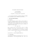
7 Methods for estimating the Early Failure Rate weibull distribution is applied to approximate the CDF of early failure period; it can exhibit a shape where the failure rate decreases over time. weibull distribution is characterized by two important parameters, scale factor ( ) and shape factor ( ). They are defined as: )(1exp1)(tRttF where t : life cycle or life time (EFR duration to failure) : scale factor or characteristic function : shape factor or shape parameter Rearranging the equation, one obtains: lnln)](1ln(ln[)](1ln[exp)(1 ttFttFttF When plotted in ln [- ln ( 1 F(t) ) ] against t on log scale (Below figure) , the data should approximately fall on a straight regression line.)
8 Scale factor can be obtained from the intercept of the straight line; it is constant for a fixed test condition. Shape factor is the slope of the straight line and its value is less than one for early failure period. Using the relationships that f(t) = dF(t)/dt and (t) = f(t)/R(t), one can derive the failure rate as: 1)( tt Figure 2 - ln t, test time (hr.) VS ln[-ln(1-F(t))] Methods for estimating the Useful Life Failure Rate When devices containing early defects have been eliminated to a certain degree, the initial failure rate becomes extremely small, and the failure rate exhibits a gradually declining curve over time.
9 The failure rate at this period is obtained by dividing the number of failures observed by the device hours, usually expressed as failures per billion device hours (FITs). This is called point estimate because it is obtained from observation on a portion (sample) of the population of devices. In order to determine the unknown population parameter from known sample statistics, it is necessary to make use of specific probability distribution . The chi-square distribution ( 2) that relates observed and expected frequencies of an event is frequently used. The relationship between failure rate at stress conditions and the chi-square distribution is shown in the following formula: tn stress2),(2 where: stress = failure rate at stress conditions 2 = chi-square function = (100 - confidence level) /100 n = degree of freedom = 2r + 2 r = number of failures t = device hours The chi-square values for equal to 60% and 90% at r between 0 and 12 are shown in below table.
10 Chi-Square distribution Function 60% Confidence Level 90% Confidence Level No. Fails 2 Quantity No. Fails 2 Quantity 0 1 2 3 4 5 6 7 8 0 1 2 3 4 5 6 7 8 Since all the Reliability tests are performed under accelerated stress condition, it is important to evaluate the acceleration factor of different stresses. 1) Thermal Acceleration Factor Acceleration factor for thermal stress is calculated using the Arrhenius equation: ][)27312731(stressTuseTkaEeAFt where: AFt = thermal acceleration factor Ea = activation energy in electron Volts (eV)1, k = Boltzmann s constant x 10-5 eV / K Tuse = junction temperature at normal use condition in C Tstress = the stress temperature in C 2) Voltage Acceleration Factor High electrical field can cause physical damage in the oxide layers.