Transcription of SEMICONDUCTOR SWITCHES REPLACE …
1 SEMICONDUCTOR SWITCHES REPLACE thyratrons ANDIGNITRONSA. Welleman, E. Ramezani, U. SchlapbachABB semiconductors AG, CH-5600 Lenzburg, SwitzerlandAbstractA solid state switching system is presented which is designed a high reliable,long life, low maintenance product for short repetitive and high di/dt pulses. Thesolid state switch uses special designed SEMICONDUCTOR devices with integrated fasttriggering circuits which are powered by one closed loop current source powersupply. Blocking voltages of over 30 kV are possible by stacking several devices inseries connection. The solid state system has no environmental restrictions and canbe used in any position1) INTRODUCTIONS ince several years ABB is offering complete solid state SWITCHES which are based on a wide range of specificdevices which are designed for non-repetitive pulsed power applications.
2 More recently, interest has been shownin fast SEMICONDUCTOR SWITCHES which can be used at medium frequencies, to REPLACE thyratrons and ignitronsbecause of longer life, no use of mercury and almost no maintenance. For this applications, ABB has designed anew platform technology and is using this concept in a range of different SWITCHES . These SWITCHES are so calledPower Parts, as they are built up as an assembly with semiconductors , drivers, clamping, cooling, power supplyand triggering, but are without cabinet or control ) SEMICONDUCTOR DEVICESThe evolution of silicon wafers for high di/dt application started about 1975 with the central gate SCR s capableto handle 200 400 A/ s, followed later by higher interdigitated gate structures which allowed about to doublethese values.
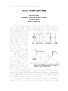
3 Since 1992 the use of GTO-like structures has improved the di/dt handling tremendous, but onlyin combination with special buffer layers and very low electron-irradiation, it was possible to develop anacceptable wafer for high current, high di/dt and repetitive switching. To reduce the inductance between switchcomponent and freewheeling diode, the last one was directly integrated on the same silicon wafer. A GTO-likewafer structure with integrated freewheeling diode is shown in Fig. 1 (right) direct next to a full switching waferwithout 1)Wafer evolution 1975 2000 for pulsed power . (Silicon size 51 mm)Additional to this improvement on wafer level, some modification on the device housing was done to get morethrough-connections through the ceramic housing to the driver unit.
4 To get the shortest possible low inductancedistance to the driver unit, the driver was built-up and integrated around the ceramic SEMICONDUCTOR this solution the inductance between switch, freewheeling diode and the driver unit can be reduced to onlya few nH. This compact component is the base of a platform technology where a family of 3 different sizes (51 /68 and 91 mm ) can be used to design switch-assemblies for different current levels and thermalrequirements. For Thyratron or Ignitron replacement normally a Reverse Conduction device will be used, butReverse Blocking or Asymmetric versions are also available. The standard blocking voltage is rated at Vdrm =4,5 kV and max.
5 Cont. DC Voltage is kV, or kV < 1 min. The switching system presented is using a 51mm reverse conducting SEMICONDUCTOR discharge switch with integrated driver unit, ABB P/N 5 SPR Fig. 2 and Fig. 2)Reverse conducting 51 mm discharge switch showing Fig. 3) Device 5 SPR 08F4500 completewafer, switching device and driver unit device 5 SPR 08F4500 can be used within a wide specification, of which the key parameters like pulsecurrent, pulse length, rep. rate and cooling are the main factors to make a reliable design. The basic specificationof the device is Vdrm = kV / Vdc max = kV / di/dt = 10 kA/ s / peak-pulse current = 10 kA @ tp =50 s / 400 )DRIVER UNIT, INTEGRATED WITH 51 mm DEVICETo reach a very low inductance the driver unit is integrated direct around the SEMICONDUCTOR switching this construction , and the very low induction gate-connection path, high di/dt and very fast switch-on canbe reached.
6 As the switching component is designed for repetitive use, the driver unit has an on-board powersupply, which needs an external power source. In case of one single device, the isolation can be easily handled,but in case of stacking several devices in series connection, galvanic separation between the driver units isgetting dominant. Therefore it was decided to equip the driver unit with an input transformer, using inductiveextraction fed by a separate current source. The current source operates with a 25 kHz closed loop, using an HV-cable, which is sloped through the input transformers of all the driver units.
7 The triggering of the switch isactivated by an optical signal. The optical receiver in the driver unit is a commercial HP optical receiver forglassfibers. The driver unit accommodates LED s which indicate Status, Power and Faillure mode. The powerconsumption of the driver unit is depending on switching frequency, which is about 4 W for up to 50 Hz and 10W for 400 )POWER SUPPLYA closed loop current source power supply is used to energize the driver units. In standard version this is donewith 25kHz / 4 A, using a closed loop high voltage cable sloped through the input transformers of the driverunits. The HV-cable has an isolation voltage of over 30 kVdc cont.
8 Therefore the series connection of devicescan easily go up to a charging voltage of 25 kVdc, which means about 10 device switching levels. For highervoltages, a master slave combination of power supplies, or isolation transformers to feed more power supplieshas to be used, and series connection of stacks has to be provided. Fig. 4 shows the power supply for the 51 4) Current Source Power Supply5)LIGHT EMITTER BOXThe driver units of the SWITCHES are activated by optical signals, which are provided by a light emitter box ( ). For simultaneous triggering of all devices, the light emitter box has the same amount of optical outputsockets as the switch assembly has devices in series connection.
9 In addition there is one optical output tomonitor the function of the box. The trigger signal provided to the box can be electrical or optical, depending onsystem requirements. It is recommended to use optical input for the trigger signal to avoid any interference byhigh electric fields in the switch area. Therefore it is also recommended to use the light emitter box away fromthe switch assembly. The pulse-length of the trigger signal is an extreme important value, as the switch needs tobe on during the full time of the main pulse. This means that if the main pulse, incl. ev. negative parts, is 20 s, the trigger pulse should be at least 30 s long, and stopped only shortly before recharging will is also shown in Fig.
10 5. The test was done over 6 device levels (15 kV) and a 12 kA pulse 5) Example for trigger pulse duration vs. main pulse Fig. 6) Light distribution box with optical cable and driver unit6) THYRATRON REPLACEMENTB ased on the circuit diagram for thyratron with freewheeling diode, ABB has designed a switch assembly, whichoffers the same performance, but is superior in handling, maintenance and lifetime 7) Circuit diagram thyratron switch Fig. 8) Circuit diagram solid state switch7) SOLID STATE SWITCH ASSEMBLYThe solid state switch assembly was designed for 12 kVdc charge voltage, using reverse conducting devices andtypical specified for I-peak = 1,5 kA / di/dt = 1,5 kA/ s / tp = 10 s and a rep.