Transcription of Simultaneous atomic-resolution electron …
1 ARTICLER eceived 22 Dec 2015|Accepted 8 Jul 2016|Published 26 Aug 2016 Simultaneous atomic - resolution electronptychography andZ-contrast imaging of lightand heavy elements in complex nanostructuresH. Yang1, Rutte2, L. Jones1, M. Simson3, R. Sagawa4, H. Ryll5, M. Huth3, Pennycook6, Green2,H. Soltau3, Y. Kondo4, Davis2& Nellist1 The aberration-corrected scanning transmission electron microscope (STEM) has emergedas a key tool for atomic resolution characterization of materials, allowing the use of imagingmodes such asZ-contrast and spectroscopic mapping. The STEM has not been regarded asoptimal for the phase-contrast imaging necessary for efficient imaging of light , recent developments in fast electron detectors and data processing capability is shownto enable electron ptychography, to extend the capability of the STEM by allowingquantitative phase images to be formed simultaneously with incoherent signals. Wedemonstrate this capability as a practical tool for imaging complex structures containing lightand heavy elements, and use it to solve the structure of a beam-sensitive carbon nanos-tructure.
2 The contrast of the phase image contrast is maximized through the post-acquisitioncorrection of lens aberrations. The compensation of defocus aberrations is also used for themeasurement of three-dimensional sample information through post-acquisition : of Materials, University of Oxford, Parks Road, OX1 3PH Oxford, of Chemistry, University of Oxford, 12 Mansfield Road, OX1 3 TAOxford, GmbH, Sckellstrasse 3, 81667 Mu nchen, Ltd 3-1-2 Musashino Akishima, Tokyo 196-8558, GmbH,Otto-Hahn-Ring 6, 81739 Mu nchen, of Physics, University of Vienna, Boltzmanngasse 5, 1090 Vienna, Austria. Correspondence andrequests for materials should be addressed to (email: or to (email: COMMUNICATIONS| 7:12532 | DOI: | an atomic - resolution image in the electronmicroscope that provides dose-efficient, high-contrastimaging of light elements, while also providing strongcompositional contrast, has been a long-standing light materials, such as graphene and biological structures,high-energy electrons are predominantly only scattered once inthe sample.))
3 Such single scattering conditions can be described asa weak-phase object (WPO)1, where only a small phase shift isintroduced to the electron wave. Phase-contrast imaging usingelectrons has been shown to provide the highest dose efficiencyfor imaging WPOs, where radiation damage is a limiting factor2,compared with inelastic electron scattering, as well as X-ray andneutron scattering. Electric and magnetic fields also lead to aphase shift of the electron beam. Phase-contrast imagingtherefore plays an important role in the imaging of biologicalstructures, light materials such as graphene and the detection ofelectric and magnetic fields. It is generally performed in theconventional transmission electron microscope (CTEM) usingeither deliberately injected lens aberrations or a phase plate3,toform image contrast of a WPO, or using off-axis holography4,5,which requires a separate reference beam deflected using anelectron a strong compositional sensitivity to elementtype, however, requires the detection of relatively high-anglescattering and this is performed using annular dark-field (ADF)imaging in the scanning TEM (STEM), as shown in Fig.
4 1, whichforms an image with atomic -number contrast (Z-contrast).A beam of electrons is focused to form a probe of atomicdimensions that is raster scanned across the sample and the ADFdetector collects the intensity of the high-angle scattering that isthen plotted as a function of probe position to form an technique has developed into a key approachfor atomic - resolution imaging, in particular as the developmentof hardware correctors for the inherent spherical aberrationof the objective lens6,7. It is an incoherent imaging technique,which means that the optimal conditions for imaging arethe smallest, most intense illuminating probe is achieved by tuning the aberration corrector for thesmallest possible aberrations. Phase-contrast imaging, however, isa coherent imaging mode and requires aberrations, such as acombination of spherical aberration and defocus, to form aneffective phase plate. Such conditions are referred to as Scherzerconditions 9. Alternative approaches that also make use ofaberrations include negative spherical aberration conditions10or the use of a focal series11in TEM.
5 The optimal conditions forincoherentZ-contrast imaging are therefore different from thosefor coherent phase contrast, thus preventing their simultaneousoptimal implementation. Furthermore, the principle ofreciprocity12shows that the formation of a conventionalphase-contrast image in STEM requires the use of a small axialbright-field (BF) detector, which collects only a small fraction ofthe transmitted electrons and is therefore dose we make use of electron ptychography to enable anefficient, quantitative phase imaging in STEM under opticalconditions that are optimized for incoherent imaging so that thephase information is recorded simultaneously with theZ-contrastimage, allowing a full analysis. Although ptychography hasbecome well established for imaging with light13and X-rays14 16,its use with electrons has been more limited. The principleof ptychography is that a camera is used to record the intensityin the STEM detector plane as a function of probe position,resulting in a four-dimensional (4D) data set (two STEM probe coordinates and two coordinates within the detectorplane), which can be used to reconstruct a phase image.
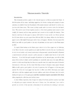
6 Initialexperimental demonstrations of electron ptychographywere limited by the camera speed, microscope stability and theavailability of sufficient computational processing power, andonly very small images (typically 32 32 pixels) could bereconstructed17. More recent demonstrations have used highlydefocused probes that illuminate a wider region of the sampleto provide a larger field of view, while still limiting the number ofprobe positions and camera frames18 20. Such defocusedprobes are incompatible with the conditions required forincoherent imaging and so cannot be used simultaneously withZ-contrast imaging. The subsequent formation of aZ-contrastimage would require refocusing of the electron probe, whichrequires further electron dose on the sample and loses theability to exactly register the phase andZ-contrast probeSpecimenADFP ixelateddetectorCarbon nanotubeADFP haseRadian3210 1 2 3+Qp+Qp Qp QpIIIIIIIIIIIIII abcdeFigure 1 | Simultaneous atomic resolution incoherent and coherent imaging.
7 (a) An ADF detector collects the dark-field signal to form (b) an incoherentZ-contrast image. (c) The Simultaneous phase image is reconstructed using ptychography. Simultaneously, a fast pixelated detector records the coherentBF diffraction pattern at every probe position forming a 4D data set. Taking the Fourier transform of the 4D data set with respect to probe position results ina complex 4D matrixG(Kf,Qp), which carries the phase information of the interference between diffracted and undiffracted beams. (d,e) An example of themodulus and phase of the complex matrixG(Kf,Qp) at a single spatial frequencyQpwhere two diffracted beams Qpand Qp(indicated by dashedlines) overlap with the undiffracted direct beam. (d) The areas labelled as area I are double-overlap regions where one diffracted beam interferes with thedirect beam and area II is the triple-overlap region where both diffracted beams and the direct beam interfere. Area III has no interfering beams and isonlynoise and is therefore not used in the ptychography reconstruction.
8 By analysing the phase information for all spatial frequencies in the image, (c) the phaseimage can be reconstructed. Scale bar, 1 COMMUNICATIONS | DOI: COMMUNICATIONS| 7:12532 | DOI: | first proof-of-principle attempt to form Simultaneous ADF andphase-contrast images21was also limited in field of view bythe camera speed. Differential phase contrast (DPC) imageshave been formed at atomic resolution in the STEM and usedto detect ferroelectric polarization22, and the importance ofadding phase-sensitive imaging as a STEM technique discussed23,but the differential approach did not offer quantitativeimage phase measurement and does not offer the possibilityof post-acquisition aberration correction demonstrated has been shown to enable phase extraction usingsignals from segmented detectors including tri-sectors24andrecently at atomic resolution using segments synthesized frompixelated data25. Large detector pixels may lead to a non-isotropictransfer of phase information with reduced phase-contrasttransfer we show that new capabilities that have been enabled byrecent developments in high-speed detector technology(described further in the Methods section) that provide framespeeds of 1 kHz or greater allowing image acquisition at scanningspeeds much closer to those typically used in STEM.
9 We showthat the combination ofZ-contrast and phase imaging reveals thestructure of a complex nanomaterial that could not be determinedusing previous methods. Ptychography also allows for furtherpost-acquisition detection and correction of residual lensaberrations, which optimizes the contrast of the phase also show that ptychographic reconstruction can be used toaccess three-dimensional (3D) information through its intrinsicoptical-sectioning acquisition and processing. Figure 1a shows a schematic ofthe optical configuration for the experiment presented here, withsingle frames of the experimental diffraction patterns shown inSupplementary Fig. 1. Further experimental details are describedin the Methods section. As a highly convergent beam is used inSTEM, the diffracted beams observed in the far field broaden intodiscs. The phase information is found where these discs a fast pixelated STEM detector, diffraction patternsconsisting of primarily the BF disc (direct beam) were recorded atevery probe position during a raster scan, thereby forming a 4 Ddata set.
10 The dark-field signal is simultaneously collected using anADF detector, to form an incoherentZ-contrast image, asshown in Fig. 1b. In the detector plane, the recorded electronmicro-diffraction patterns as a function of scattering vectorKfand probe positionR0, can be described as the Fourier transformof product of the probeP(R R0) and the specimen transmissionfunctioncR ,MKf;R0 ZPR R0 cR expi2pKf R dR 1 The intensity of the diffraction patternMKf;R0 jj2is recordedbut the phase is lost. Various ptychography approaches inelectron and X-ray microscopy have been developed. Herewe used the Wigner distribution deconvolution (WDD)approach described by Rodenburg and Bates27, anddemonstrated experimentally using X-rays28. WDD isnon-iterative and therefore fast, especially under the conditionspresented here where 256 256 image pixels results in 65,536individual diffraction patterns to be processed. Iterativeapproaches14,18,29 31and direct inversion methods19havealso been developed, but as yet they have not beendemonstrated on the type of atomic -scale focused probe dataused here, to enable the Simultaneous incoherent feasibility of using iterative methods on this type of datawill be explored in further is performed by taking the forward Fourier transform ofMKf;R0 jj2in equation (1) with respect to the probe positionsR0, leading to a complex 4D matrix denoted asG(Kf,Qp),27 GKf;Qp AKf A Kf Qp KfCKf C Kf Qp 2 where Kfdenotes a convolution with respect to the scatteringvectorKfand the two termsAKf A Kf Qp andCKf C Kf Qp are functions of the probe formingaperture,A(Kf), and the specimen transmission function,CKf , respectively.