Transcription of Small Signal Zener Diodes - Vishay Intertechnology
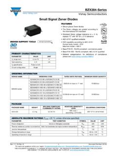
1 BZT52- series Vishay Semiconductors Small Signal Zener Diodes FEATURES. Silicon planar Zener Diodes Available The Zener voltages are graded according to the international E24 standard AEC-Q101 qualified available ESD capability according to AEC-Q101: . Human body model > 8 kV . Machine model > 800 V. DESIGN SUPPORT TOOLS click logo to get started Base P/N-E3 - RoHS-compliant, commercial grade Models Base P/N-HE3 - RoHS-compliant, AEC-Q101 qualified Available Material categorization: for definitions of compliance PRIMARY CHARACTERISTICS please see PARAMETER VALUE UNIT. VZ range nom. to 75 V. Test current IZT ; 5 mA. VZ specification Pulse current Circuit configuration Single ORDERING INFORMATION. DEVICE NAME ORDERING CODE TAPED UNITS PER REEL MINIMUM ORDER QUANTITY. BZT52C2V4-E3-08 to BZT52C75-E3-08. BZT52B2V4-E3-08 to BZT52B75-E3-08. 3000 (8 mm tape on 7" reel) 15 000/box BZT52C2V4-HE3-08 to BZT52C75-HE3-08.
2 BZT52B2V4-HE3-08 to BZT52B75-HE3-08. BZT52- series BZT52C2V4-E3-18 to BZT52C75-E3-18. BZT52B2V4-E3-18 to BZT52B75-E3-18. 10 000 (8 mm tape on 13" reel) 10 000/box BZT52C2V4-HE3-18 to BZT52C75-HE3-18. BZT52B2V4-HE3-18 to BZT52B75-HE3-18. PACKAGE. MOLDING COMPOUND MOISTURE SENSITIVITY. PACKAGE NAME WEIGHT SOLDERING CONDITIONS. FLAMMABILITY RATING LEVEL. MSL level 1. SOD-123 mg UL 94 V-0 260 C/10 s at terminals (according J-STD-020). ABSOLUTE MAXIMUM RATINGS (Tamb = 25 C, unless otherwise specified). PARAMETER TEST CONDITION SYMBOL VALUE UNIT. Diode on ceramic substrate mm;. Ptot 500 mW. 5 mm2 pad areas Power dissipation Diode on ceramic substrate mm;. Ptot 410 mW. mm2 pad areas Zener current See table Electrical Characteristics . Valid provided that electrodes are kept at Thermal resistance junction to ambient air RthJA 300 K/W. ambient temperature Junction temperature Tj 150 C.
3 Storage temperature range Tstg -65 to +150 C. Operating temperature range Top -55 to +150 C. Rev. , 20-Feb-18 1 Document Number: 85760. For technical questions within your region: THIS DOCUMENT IS SUBJECT TO CHANGE WITHOUT NOTICE. THE PRODUCTS DESCRIBED HEREIN AND THIS DOCUMENT. ARE SUBJECT TO SPECIFIC DISCLAIMERS, SET FORTH AT BZT52- series Vishay Semiconductors ELECTRICAL CHARACTERISTICS (Tamb = 25 C, unless otherwise specified). Zener VOLTAGE TEST REVERSE DYNAMIC TEMP. ADMISSABLE Zener . RANGE (1) CURRENT VOLTAGE RESISTANCE COEFFICIENT CURRENT (4). PART MARKING ZZ at ZZK at IZ at IZ at VZ at IZT1 IZT1 IZT2 VR at IR VZ. NUMBER CODE IZT1 IZT2 Tamb = 45 C Tamb = 25 C. V mA V nA 10-4/ C mA. MIN. NOM. MAX. BZT52C2V4 W1 5 1 - - 85 600 -9 to -4 - - BZT52C2V7 W2 5 1 - - 75 (< 83) < 500 -9 to -4 113 134. BZT52C3V0 W3 5 1 - - 80 (< 95) < 500 -9 to -3 98 118. BZT52C3V3 W4 5 1 - - 80 (< 95) < 500 -8 to -3 92 109.
4 BZT52C3V6 W5 5 1 - - 80 (< 95) < 500 -8 to -3 85 100. BZT52C3V9 W6 5 1 - - 80 (< 95) < 500 -7 to -3 77 92. BZT52C4V3 W7 4 5 1 - - 80 (< 95) < 500 -6 to -1 71 84. BZT52C4V7 W8 5 5 1 - - 70 (< 78) < 500 -5 to +2 64 76. BZT52C5V1 W9 5 1 > 100 30 (< 60) < 480 -3 to +4 56 67. BZT52C5V6 WA 6 5 1 >1 100 10 (< 40) < 400 -2 to +6 50 59. BZT52C6V2 WB 5 1 >2 100 (< 10) < 200 -1 to +7 45 54. BZT52C6V8 WC 5 1 >3 100 (< 8) < 150 +2 to +7 41 49. BZT52C7V5 WD 7 5 1 >5 100 4 (< 7) < 50 +3 to +7 37 44. BZT52C8V2 WE 5 1 >6 100 (< 7) < 50 +4 to +7 34 40. BZT52C9V1 WF 5 1 >7 100 (< 10) < 50 +5 to +8 30 36. BZT52C10 WG 10 5 1 > 100 (< 15) < 70 +5 to +8 28 33. BZT52C11 WH 11 5 1 > 100 6 (< 20) < 70 +5 to +9 25 30. BZT52C12 WI 12 5 1 >9 100 7 (< 20) < 90 +6 to +9 23 28. BZT52C13 WK 13 5 1 > 10 100 9 (< 25) < 110 +7 to +9 21 25. BZT52C15 WL 15 5 1 > 11 100 11 (< 30) < 110 +7 to +9 19 23.
5 BZT52C16 WM 16 5 1 > 12 100 13 (< 40) < 170 +8 to + 17 20. BZT52C18 WN 18 5 1 > 14 100 18 (< 50) < 170 +8 to + 15 18. BZT52C20 WO 20 5 1 > 15 100 20 (< 50) < 220 +8 to +10 14 17. BZT52C22 WP 22 5 1 > 17 100 25 (< 55) < 220 +8 to +10 13 16. BZT52C24 WR 24 5 1 > 18 100 28 (< 80) < 220 +8 to +10 11 13. BZT52C27 WS 27 5 1 > 20 100 30 (< 80) < 250 +8 to +10 10 12. BZT52C30 WT 28 30 32 5 1 > 100 35 (< 80) < 250 +8 to +10 9 10. BZT52C33 WU 31 33 35 5 1 > 25 100 40 (< 80) < 250 +8 to +10 8 9. BZT52C36 WW 34 36 38 5 1 > 27 100 40 (< 90) < 250 +8 to +10 8 9. BZT52C39 WX 37 39 41 5 1 > 29 100 50 (< 90) < 300 +10 to +12 7 8. BZT52C43 WY 40 43 46 5 1 > 32 100 60 (< 100) < 700 +10 to +12 6 7. BZT52C47 WZ 44 47 50 5 1 > 35 100 70 (< 100) < 750 +10 to +12 5 6. BZT52C51 X1 48 51 54 5 1 > 38 100 70 (< 100) < 750 +10 to +12 5 6. BZT52C56 X2 52 56 60 - - < 135 (2) < 1000 (3) typ.
6 +10 (2) - - BZT52C62 X3 58 62 66 - - < 150 (2) < 1000 (3) typ. +10 (2) - - BZT52C68 X4 64 68 72 - - < 200 (2) < 1000 (3) typ. +10 (2) - - BZT52C75 X5 70 75 79 - - < 250 (2) < 1500 (3) typ. +10 (2) - - Notes IZT1 = 5 mA, IZT2 = 1 mA. (1) Measured with pulses t = 5 ms p (2) I. ZT1 = mA. (3) I. ZT2 = mA. (4) Valid provided that electrodes are kept at ambient temperature Rev. , 20-Feb-18 2 Document Number: 85760. For technical questions within your region: THIS DOCUMENT IS SUBJECT TO CHANGE WITHOUT NOTICE. THE PRODUCTS DESCRIBED HEREIN AND THIS DOCUMENT. ARE SUBJECT TO SPECIFIC DISCLAIMERS, SET FORTH AT BZT52- series Vishay Semiconductors ELECTRICAL CHARACTERISTICS (Tamb = 25 C, unless otherwise specified). Zener VOLTAGE TEST REVERSE DYNAMIC TEMP. ADMISSABLE Zener . RANGE (1) CURRENT VOLTAGE RESISTANCE COEFFICIENT CURRENT (4). PART MARKING ZZK at IZ at IZ at VZ at IZT1 IZT1 IZT2 VR at IR ZZ at IZT1 VZ.
7 NUMBER CODE IZT2 Tamb = 45 C Tamb = 25 C. V mA V nA 10-4/ C mA. MIN. NOM. MAX. BZT52B2V4 W1 5 1 - - 85 600 -9 to -4 - - BZT52B2V7 W2 5 1 - - 75 (< 83) < 500 -9 to -4 113 134. BZT52B3V0 W3 5 1 - - 80 (< 95) < 500 -9 to -3 98 118. BZT52B3V3 W4 5 1 - - 80 (< 95) < 500 -8 to -3 92 109. BZT52B3V6 W5 5 1 - - 80 (< 95) < 500 -8 to -3 85 100. BZT52B3V9 W6 5 1 - - 80 (< 95) < 500 -7 to -3 77 92. BZT52B4V3 W7 5 1 - - 80 (< 95) < 500 -6 to -1 71 84. BZT52B4V7 W8 5 1 - - 70 (< 78) < 500 -5 to +2 64 76. BZT52B5V1 W9 5 5 1 > 100 30 (< 60) < 480 -3 to +4 56 67. BZT52B5V6 WA 5 1 >1 100 10 (< 40) < 400 -2 to +6 50 59. BZT52B6V2 WB 5 1 >2 100 (< 10) < 200 -1 to +7 45 54. BZT52B6V8 WC 5 1 >3 100 (< 8) < 150 +2 to +7 41 49. BZT52B7V5 WD 5 1 >5 100 4 (< 7) < 50 +3 to +7 37 44. BZT52B8V2 WE 5 1 >6 100 (< 7) < 50 +4 to +7 34 40. BZT52B9V1 WF 5 1 >7 100 (< 10) < 50 +5 to +8 30 36. BZT52B10 WG 10 5 1 > 100 (< 15) < 70 +5 to +8 28 33.
8 BZT52B11 WH 11 5 1 > 100 6 (< 20) < 70 +5 to +9 25 30. BZT52B12 WI 12 5 1 >9 100 7 (< 20) < 90 +6 to +9 23 28. BZT52B13 WK 13 5 1 > 10 100 9 (< 25) < 110 +7 to +9 21 25. BZT52B15 WL 15 5 1 > 11 100 11 (< 30) < 110 +7 to +9 19 23. BZT52B16 WM 16 5 1 > 12 100 13 (< 40) < 170 +8 to + 17 20. BZT52B18 WN 18 5 1 > 14 100 18 (< 50) < 170 +8 to + 15 18. BZT52B20 WO 20 5 1 > 15 100 20 (< 50) < 220 +8 to +10 14 17. BZT52B22 WP 22 5 1 > 17 100 25 (< 55) < 220 +8 to +10 13 16. BZT52B24 WR 24 5 1 > 18 100 28 (< 80) < 220 +8 to +10 11 13. BZT52B27 WS 27 5 1 > 20 100 30 (< 80) < 250 +8 to +10 10 12. BZT52B30 WT 30 5 1 > 100 35 (< 80) < 250 +8 to +10 9 10. BZT52B33 WU 33 5 1 > 25 100 40 (< 80) < 250 +8 to +10 8 9. BZT52B36 WW 36 5 1 > 27 100 40 (< 90) < 250 +8 to +10 8 9. BZT52B39 WX 39 5 1 > 29 100 50 (< 90) < 300 +10 to +12 7 8. BZT52B43 WY 43 5 1 > 32 100 60 (< 100) < 700 +10 to +12 6 7.
9 BZT52B47 WZ 47 5 1 > 35 100 70 (< 100) < 750 +10 to +12 5 6. BZT52B51 X1 50 51 52 5 1 > 38 100 70 (< 100) < 750 +10 to +12 5 6. BZT52B56 X2 56 - - < 135 (2) < 1000 (3) typ. +10 (2) - - BZT52B62 X3 62 - - < 150 (2) < 1000 (3) typ. +10 (2) - - BZT52B68 X4 68 - - < 200 (2) < 1000 (3) typ. +10 (2) - - BZT52B75 X5 75 - - < 250 (2) < 1500 (3) typ. +10 (2) - - Notes IZT1 = 5 mA, IZT2 = 1 mA. (1) Measured with pulses t = 5 ms p (2) I. ZT1 = mA. (3) I. ZT2 = mA. (4) Valid provided that electrodes are kept at ambient temperature Rev. , 20-Feb-18 3 Document Number: 85760. For technical questions within your region: THIS DOCUMENT IS SUBJECT TO CHANGE WITHOUT NOTICE. THE PRODUCTS DESCRIBED HEREIN AND THIS DOCUMENT. ARE SUBJECT TO SPECIFIC DISCLAIMERS, SET FORTH AT BZT52- series Vishay Semiconductors TYPICAL CHARACTERISTICS (Tamb = 25 C, unless otherwise specified). mA . 103 100.
10 TJ = 25 C. 102 5. 4. IF 10 3. rzj 33. TJ = 100 C 2. 1 27. 22. 10-1 10 18. TJ = 25 C. 10-2 5. 15. 4. 12. 10-3 3. 10. 2. 10-4 10 -5 1. 0 1V 2 5 1 2 5 10 2 5 100 mA. 18114 VF 18119 IZ. Fig. 1 - Forward characteristics Fig. 4 - Dynamic Resistance vs. Zener Current mW . 500 103. 7 Tj = 25 C. 5. 400 4. Rzj 3 47 + 51. Ptot 43. 2 39. 300 36. 102. 7. 200. 5. 4. 3. 100. 2. 0 10. 0 100 200 C 2 3 4 5 1 2 3 4 5 10. 18120 IZ mA. 18888 Tamb Fig. 2 - Admissible Power Dissipation vs. Ambient Temperature Fig. 5 - Dynamic Resistance vs. Zener Current . 103. 1000 VZ. TJ = 25 C 5 Rzth = RthA x VZ x 5. 4. 4 Tj 3. 3. 2. rzj 2 Rzth 100 102. 5 5. 4 4. 3 3. 2 2. 10 10. 5. 5. 4 4. 3 3. 2. negative positive 2. 1 1. 2 5 1 2 5 10 2 5 100 mA 1 2 3 4 5 10 2 3 4 5 100 V. 18117 IZ 18121 VZ at IZ = 5 mA. Fig. 3 - Dynamic Resistance vs. Zener Current Fig. 6 - Thermal Differential Resistance vs.