Example: confidence
Smoltek extends evaluation agreement with global ...
Jan 03, 2022 · semiconductor industry within the Group company Smoltek Semi. Initially, the focus is on industrializing the company's extremely small and thin CNF-MIM capacitors, where two separate agreements for industrial evaluation were signed in the spring of 2020. One of these agreements was
Tags:
Information
Domain:
Source:
Link to this page:
Documents from same domain

+49 (0) 89-1241498-40 sales@amkor
www.semiconductorpackagingnews.comAmkor Technology, Inc. a leading provider of semiconductor packaging, assembly and test services to the world's leading semiconductor companies and electronics OEMs, announces the opening of its German sales office in Munich.

NANIUM introduces WLCSP+ An advanced …
www.semiconductorpackagingnews.comNANIUM introduces WLCSP+ An advanced solution powered by Fan-Out Technology Vila do Conde, Porto, Portugal – 27th May 2015 – NANIUM S.A., acknowledged for its experience in designing and developing reliable, innovative semiconductor packaging solutions, announced the

CyberOptics to Deliver Technical Presentation About the ...
www.semiconductorpackagingnews.comInspection Is ecoming Essential in Advanced Packaging [ in the AP technical track on December 2nd at 3:30pm local time. Advanced Packaging continues to be among the most dynamic and rapidly evolving areas of semiconductor development and manufacturing. Most of these new processes take advantage of

Wafer-Level Packaging Symposium (WLPS) Program …
www.semiconductorpackagingnews.comDec 20, 2021 · Wafer-Level Packaging Symposium (WLPS) Program Announced and Registration Now Open Minneapolis, MN – The SMTA is pleased to announce the technical program for the Wafer-Level Packaging Symposium (WLPS). The symposium will be held February 15-17, 2022 at the DoubleTree by Hilton Hotel in San Jose, California.
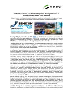
SEMICON Southeast Asia 2022 to take place in Penang with a ...
www.semiconductorpackagingnews.comIndustry leaders from the semiconductor ecosystem to address sustainability challenges and supply chain disruption through green factories and advanced manufacturing systems Penang, Malaysia, December 6, ... snowball into longer lead times for chip production if the industry sticks to the current status quo. We

MacDermid Inc. 245 Freight Street, Waterbury, CT 06702 USA
www.semiconductorpackagingnews.comThe Enthone brand MICROFAB EVF NiBAR, a boric acid free sulfamate nickel electroplating process for semiconductor applications and ATROX CF200-1D an electrically conductive die attach film with thermal conductivity of >20 W/m-K will be promoted. The Compugraphics brand will showcase their complete line of photomask solutions and support services.
FOR IMMEDIATE RELEASE Press Release
www.semiconductorpackagingnews.comDec 24, 2021 · in a variety of advanced packages such as memory cards, chip carriers, hybrid circuits and multi-chip modules. It is designed for high production and an environment where process speed and thermal dissipation are key concerns. For more information on YINCAE’s SMT 88UL2 underfill, or to learn more about the YINCAE

Sondrel explains the vital coordinating role of Systems ...
www.semiconductorpackagingnews.comJan 14, 2022 · architecture design by modelling the proposal and evaluating known or reference use cases, dynamically allowing the system topology to be defined and provisioning of resources to be allocated (memory, bus fabric data/control paths, etc.). While it allows aspects of the functionality to be evaluated and validated (connectivity,
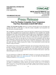
Dr. Jennie Hwang to address “Preventing Manufacturing ...
www.semiconductorpackagingnews.comJan 14, 2022 · News Release Dr. Jennie Hwang to address “Preventing Manufacturing Defects and Product Failure” and “Reliability of Electronics - the Role of Intermetallic Compounds” at IPC APEX on Monday, January 24, 2022, from 8:00AM to 11:00AM and from 3:30PM to 6:30PM, respectively. Under today’s manufacturing and market environment, the effort to maximize …
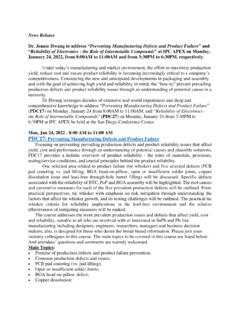
News Release
www.semiconductorpackagingnews.comJan 12, 2022 · UV-8300T - a thixotropic, damming material with very low CTE. UV 5403S is a slightly thixotropic material that can be injected as a fill adhesive, used as damming material or as a glob top. All these advanced polymers are low ion /high purity and halogen free as well as ...
Related documents
High-End Performance Packaging: 3D/2.5D ... - i-Micronews
s3.i-micronews.comdefinition for high–end performance packaging within semiconductor industry. If distinct advanced packaging technologies, including flip-chip, embedded die, 2.5D Si interposers, 3D-IC, fan-in, fan-out and hybrid bonding, are considered as high-end performance packaging, then this will be over generalizing high–end performance packaging.

2. Semiconductor Market Outlook Mr. Clark TSENG SEMI
semi.organd packaging facilities Overall Materials market flat in 2020 with wafer fab material expected to decline 0.5% while packaging materials to grow 2% Expect ~6% growth to set a record high in 2021 surpassing $55B Total Semiconductor Materials Market Stable 2020 and Record 2021 Source: SEMI Materials Market Data Subscription, September 2020 $0 ...

Advanced Packaging Current Trends & Challenges - SIA
www.semiconductors.orgPackaging revenue will almost equal to traditional packaging revenue by 2025. In 2019, the AP market share was 42.6%. Due to strong momentum in AP market driven by mega trends, the share of AP in the total semiconductor market is increasing continuously and will reach almost 50% of the market by 2025.

Taking Stock of China’s Semiconductor Industry
www.semiconductors.orgsemiconductor manufacturing equipment, and semiconductor materials. Chinese foundries currently ... It is already a global leader in outsourced assembly, packaging, and testing (OSAT). China’s leading OSAT players are ranked among the top 10 OSAT companies in the world,

The United States Innovation and Competition Act of 2021
www.democrats.senate.govadvanced packaging, and R&D facilities in the U.S. Provided support for domestic microelectronics industry, including new R&D programs at the Department of Defense. Authorized a multilateral semiconductor fund to support the adoption of a secure semiconductor supply chain and greater alignment of export control and other related

2N4401 General Purpose Transistors - Farnell
www.farnell.comdownload the ON Semiconductor Soldering and Mounting Techniques Reference Manual, SOLDERRM/D. See detailed ordering and shipping information in the package ... including part orientation and tape sizes, please refer to our Tape and Reel Packaging …

QRE1113, QRE1113GR, QRE1114GR Miniature ... - ON …
www.onsemi.comON Semiconductor reserves the right to make changes without further notice to any products herein. ON Semiconductor makes no warranty, representation or guarantee regarding the suitability of its products for any particular purpose, nor does ON Semiconductor assume any liability arising out of the application or use of any product or circuit ...
FOR IMMEDIATE RELEASE Press Release
www.semiconductorpackagingnews.comFOR ADDITIONAL INFORMATION CONTACT: Phone: (518) 452-2880 E-mail: [email protected] YINCAE Advanced Materials, LLC 19 Walker Way, Albany, NY 12205