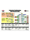
Transcription of SMT Troubleshooting Guide - Solder World
1 Le of ContentsBridgin g3In suf ficien t Fill7In suf ficien t Solder8Ra ndo m Sol de r Ball s9So lder Spat ter ing11 Mid-C hi p Solder Balls12 Tom bst oning14 Voi di ng15 BGA Head -o n-P illo w17Gr ainy Jo ints19Co oks on Ele ctr on ic sTr ou ble shooting Gui deWith this eas y-t o-useTroubl eshoot in g Guide ,you canlearn to trou bl es hoot commonSMT issues. Aft er usingit a fewtimes,it wi ll bec ome an essentialco mpanionfor you and any onein your company responsibleforoperating an SM T lin Guid e offe rs troubleshoot ingad vice for commonSMT assemblyiss ues by proc es s defect. If youriss ue is not re solv ed after follow-ing the ste ps to help identifyth epo ss ibl e root caus e and solut io n,pl ea se co nta ct your CooksonElec tron ics rep re sentative whowil l be abl e to provideyou wit hfu rther ass is ta nce.
2 Ks on Con fi de ntial For Authori zed Use OnlyBr idg ingPossibleCaus es : PCBD escriptionSM D pads wi ll co ntributeto cop lan ari ty issue re sult -ing in poor ga sket ingdurin g pri nte r se tu ghly rec omm end edto remov e so lder maskbetw een adja cent pad sesp ecia lly for fin e-pi tchcom pon en tsPossibleCaus es : Ste ncilDescriptionDir ty ste ncil with pasteunde rn eat h wi ll con tam -inate th e bar e bo ard onth e ne xt pr int, at tribu tinga pote ntia l bri en cil tensi onApe rtu re De sig nRecommendations Veri fyzer opr intgapsetup . Ensur e min imum pri ntpres sure . Incr eas e wip e fr equency. Use diff erent cle aningchemi cal re stenc il tensi on isti ght . Poo r sten ci l tensi onwil l ma ke it impo ss ibl eto ha ve a goo d setup forcons istent pri nt defini tio fine pitc h co mpo nent,it is hi ghl y re com mende dto ha ve the op eningsli ght ly sma ller tha nlan ding padsizetoimpro veste ncil to PCB gas ke ting.
3 De fini tio n:So lder connecting,in most cases, miscon -ne cti ng two or more adj acent pa ds that come intoco nt act to form a conductive pa idg ingPossibleCaus es : ScreenPrinterDescriptionPoor gas ket ing pasteooze s out ben ea th sten cildurin g pri nti ng , increasingcha nc e of we t so lderpa st e brid gesMis alig ned pr int willcha llen ge the paste topull bac k to pads du ringmolt en sta ge, increasin gth e pote nt ial fo r ear ing and bri dgingphen ome no n on the nextpr int ed bo ar d af ter stencilcle anin g op er at ionPoor print de fi nit ion withdog ears esp ecia lly onfi ne-p itc h co mponen tsDe nte d squeegee bladescould re sult in une ve npr int pr essur Zer o print gap bet weensten ci l and PCB Chec k pa st e sme arund ern ea th sten ci l.
4 Chec k suf ficient ste nci lten sur e pri nt accu racy andco nsi ste nc y for bo th pr intst rokes . Veri fy ste nc il is dr y aft erclea ni ng and bef ore nextprint. Sta nd ard clean ing modeis wet /va cuu m/ dr y. Chec k bo ar d supp or t. Adjus t sepa ra ti on spe edto achi ev e mi ni mum dogear : Dif fer ent pasteche mis tr y requ ire sdif fere nt sep ar ationspe ed to min imizedo g ea ec k sq uee ge e bla desco idg ingPossibleCaus es : ComponentPlac em entDescriptionPlac emen t ina ccu racy willna rrow the gap betwe enpa ds , inc rea sin g thecha nc e of bri ce ssi ve com pone ntpl ac eme nt pressure willsqu ee ze pa ste out ofpa ds .Recommendations Veri fy com po ne ntplac eme nt pr es sur e. Use X- ray to ve rify BGAplac eme nt . Usemicro sc ope for QFP s.
5 Veri fy ac tua l com pone nthei ght agai ns t da taent er ed in the mach ine Compo nen t pla ce menthei ght sho uld be 1 /3of paste hei gh es : ReflowProfi leDescriptionEx ten de d soa k will inpu tmor e heat to the pasteand res ul t in pa ste ho tslu mp pheno men opt a stra igh t ra mp tosp ike pro file, without soa kzon e if possibl es : SolderPas teDescriptionDr y pas te pheno me non irr eg ular pr int sh ape andincon sistent print vo lumePas te oo zes ou t of pads,ma y for m con nect ion withadjac en t pad Past e expi ry Oper at ing tem per atu rewithin suppl ier s re com -men dat ion s. Chec ktem per atu re ins ideprinter. Norm al requ ire-men t aro un d 25 C,50% RH Do not mix usi ng ne wand ol d pa ste . Oper at ing tem per atu rewithin suppl ier s re com -men dat ion s Veri fy wi th ano the r bat chof paste to conf irm pr ob -lem is batc h-r elate d.
6 Perf orm co ld and hotslum p tes t res ul t usi ngIPC-TM -65 0 Met .3 idg Fi llPossibleCaus es : Ste ncilDescriptionPas te scoop ing eff ectesp ec ially on larg e padsRecommendationsSegm ent the largeopeni ng into sma lleraper tur te do es no t roll intoapert ureRecommendations Reduc e pri nt spee d. Incr ea se pr int pr essur e. Adopt lower sque ege econt act pr int . Ensu re pa ste is notexp ired or dr y. Ensu re suff ici en t boar dsupp ort. Reduc e sq ueegeepres sure .300 mDe fini tio n:Amo unt of Solder past e deposi ted onPWB at pr int er stat ion is much less than ste ncilope ning des es : Sol derDe fini tio n:Am ount of Solder pa st e deposite d on PWBat printe r st atio n is much less tha n st encil open ingde sig n or, af ter reflow, insufficient sol de r to form a filletat the lder paste ad heres onth e sten ci l aper tur e wallsRecommendations Area ratio > 6 Aspec t rat io > No bur r on ste ncilaper tur e edgePossibleCaus es : Ste ncilDescriptionPrin t defin itionsRecommendations Veri fy pri nt setup Reduc e pri nt spee d toprovi de suf ficient timefor pas te to ro ll intoaper tur es.
7 ScreenPrinterDescriptionMis mat ch in CT E betwe encomponent and PCB cancau se sol der wi cki ng ef fectwh ich may look likeinsuffic ient sol der on Atta ch th er moc oupl e oncompo nen t an d PCB. Apply so ak pr ofi le tomini mi ze del ta T be for eref low zon e. Set botto m zo ne s to behigher tem per atu re ifpossible, to kee p PCBhott er than compone ntlea es : ReflowProfi leDescriptionSo lder paste viscosityRecommendationsCh ec k pa ste condi ti onssu ch as dry pa st ephen ome no n by ver ifyi ngif paste rolls or skids alon gpri nt dire cti es : SolderPas ndo m Solder Bal lsDe fini tio n:Aft er reflow, smal l sphe ri cal particles withva ri ou s diametersar e for med away from the mainsol der poo te stu ck und er theste nc il wil l be transf erre don to th e sol der mask ofth e ne xt Veri fy zer o pr int gap se tup.
8 Chec k minimum pri ntpres sur e us ed. Chec k clea ni ng effi cie ncysuch as wet /dr y/va cuu m. Chec k wipe frequ ency .PossibleCaus es : Ste ncilDescriptionFa st ra mp-up rat e orpr eh eat rat e will notall ow suff icie nt ti me forth e sol ve nt to va po ri zeof f gradua ow preh ea t rat e isre com men de d, ty pi ca lly< 1. 5 C/se c from roomte mp era tur e to 150 es : ReflowProfi leDescriptionTr app ed moi st ur e mayre sult in exp losivevapor izati peci al ly for lowe r gra dePC Bs suc h as FR2 , CEM 1,te nd s to abso rb moist ur ke 12 0 C for 4 hour s ifne ce ssa es : PCB Mois tu pe ci ally fo r wa ter-so lub le sol der paste whichis hy gros cop ic, it tends toha ve limited ste ncil lif ebec aus e of mo ist ureabsor Minimize expo su re time Printe r tem per at ur e andhum idity to be with inrec omme nda ti on Try ne wlot of Solder pasteto ver ify pas te int egr ity.
9 Use coa rse r po wder si zeif possi ble as fine po wdersize has mo re oxi des andten ds to slump mor erea es : SolderPas teRa ndo m Solder Bal ld er Sp atteringDe fini tio n:So lder Spa tter phe nom enon is ve ry similarto sol de r balli ng, but the conce rn is usually about solderde po sit ed onto Au finger ling of bo ar dsBa re boar dscont amina tio nRecommendations Do not mix clean andwas hed bo ards . Open fresh PCBs fr ompackag e wh en rea dyto run . Ensu re worki ng ar ea isclea ne d tho ro ugh ly andnot co nta minat ed wi thsolder pas te re ma t bar e PCB s toca ptur e an d filte r solderfo und on ba re PCB befor epri nt ing stat es : PCBD escriptionIneff ec tive cl ea nin g ofste nc il wip e will tran sf ersmall par ticle s of solde ron to th e top sur fa ce ofth e ne xt ba re bo Ensu re wipe freque ncy isset co rrec tl y.
10 Use ef fec tive sol ven t,pref era bly SC10 . Use pri nt er ma chi necame ra to ins pec t theeffe cti vene ss of ste nci lclea ni ng .PossibleCaus es : ScreenPrinterDescriptionCont rol the fl ux out -ga ss ing rate to minimizeexp losiv e so lder scatteron Au pad r SA C 305 , se t slowra mp rat e of 0. 3-0. 4 C/se cfr om 21 7-2 21 C .PossibleCaus es : ReflowProfi Sold er Ba lls (M CSB)De fini tio n:Af ter refl ow, large solde r ball(s) is/arelocat ed on the side of the chip com pone nts, betwe enth e term inati ons and awa y fr om the lder di ssocia tion anddoe s not ad her e on so lderma sk .Recommendations Remo ve sol der maskbetw ee n pads . Gap bet we en pad an dsolder mas k is rec om -men ded to mainta in atlea st 75 m ~10 0 m ,pref era bly >1 20 m.