Transcription of SN54/74LS375 4-BIT D LATCH - skot9000
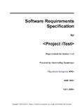
1 5-1 FAST AND LS TTL DATA4-BIT D LATCHThe sn54 / 74ls375 is a 4-BIT D-Type LATCH for use as temporary storagefor binary information between processing limits and input /output or indicatorunits. When the Enable (E) is HIGH, information present at the D input will betransferred to the Q output and, if E is HIGH, the Q output will follow the E goes LOW, the information present at the D input prior to its setup timewill be retained at the Q DIAGRAM DIP (TOP VIEW)NOTE:The Flatpak versionhas the same pinouts(Connection Diagram) asthe Dual In-Line ,3Q2Q2D2Q0Q0E0,1Q1Q1D1 GNDTRUTH TABLE(Each LATCH )NOTES:t = bit time before enabletntn+1tn = bit time before enablenegative-going +1 = bit time after enablenegative-going NAMESLOADING (Note a)HIGHLOWD1 D4 Data 1 Enable Input Latches 0, 3 Enable Input Latches 2, Q4 LATCH Outputs (Note b)10 ( ) Q4 Complimentary LATCH Outputs (Note b)10 ( ).
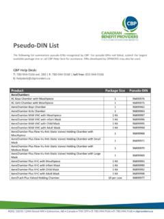
2 A) 1 TTL Unit Load ( ) = 40 A mA ) The Output LOW drive factor is 25 for Military (54) and 5 for Commercial (74)Temperature DIAGRAMDATAENABLETO OTHER LATCHQQSN54/74LS3754-BIT D LATCHLOW POWER SCHOTTKYORDERING INFORMATIONSN54 LSXXXJC eramicSN74 LSXXXNP lasticSN74 LSXXXDSOICJ SUFFIXCERAMICCASE 620-09N SUFFIXPLASTICCASE 648-08161161161D SUFFIXSOICCASE 751B-03 LOGIC SYMBOLVCC = PIN 16 GND = PIN 817 915412236510 1114 13D0D1D2D3E0,1E2,3Q0Q1Q2Q35-2 FAST AND LS TTL DATASN54/74LS375DC CHARACTERISTICS OVER OPERATING TEMPERATURE RANGE (unless otherwise specified)SblPLimitsUiTCdi iSymbolParameterMinTypMaxUnitTest ConditionsVIHI nput HIGH Input HIGH Voltage forAll InputsVILI nput LOW Input LOW Voltage forVILI nput LOW InputsVIKI nput Clamp Diode Voltage = MIN, IIN = 18 mAVOHO utput HIGH = MIN, IOH = MAX, VIN = VIHVOHO utput HIGH ,OH,INIHor VIL per Truth TableVOLO utput LOW Voltage54, = mAVCC = VCC MIN,VIN=VILor VIHVOLO utput LOW = mAVIN = VIL or VIHper Truth TableIIHI nput HIGH CurrentD InputE Input2080 AVCC = MAX, VIN = VIIHI nput HIGH CurrentD InputE = MAX, VIN = VIILI nput LOW CurrentD InputE Input = MAX, VIN = VIOSS hort Circuit Current (Note 1) 20 100mAVCC = MAXICCP ower Supply Current12mAVCC = MAXNote 1.
3 Not more than one output should be shorted at a time, nor for more than 1 CHARACTERISTICS (TA = 25 C, VCC = V)SblPLimitsUiTCdi iSymbolParameterMinTypMaxUnitTest ConditionstPLHtPHLP ropagation Delay, Data to Delay, Data to = VtPLHtPHLP ropagation Delay, Enable to Q15142725nsCCCL = 15 pFtPLHtPHLP ropagation Delay, Enable to AND LS TTL DATASN54/74LS375Q (SN54LS/ 74ls375 ONLY)DATAENABLETO OTHER LATCHQLOGIC DIAGRAMGUARANTEED OPERATING RANGESS ymbolParameterMinTypMaxUnitVCCS upply Ambient Temperature Range5474 550252512570 CIOHO utput Current High54, 74 Current SETUP REQUIREMENTS (TA = 25 C, VCC = V)SblPLimitsUiTCdi iSymbolParameterMinTypMaxUnitTest ConditionstWEnable Pulse Width20nsV50 VtsSetup Time20nsVCC = VthHold VtPLHtPLHtPLHtPLHtPHLtPHLtPHLtPHLtsthAC WAVEFORMSDEFINITION OF TERMSSETUP TIME (ts) is defined as the minimum time requiredfor the correct logic level to be present at the logic input prior tothe clock transition from LOW-to-HIGH in order to be recog-nized and transferred to the TIME (th) is defined as the minimum time followingthe clock transition from LOW-to-HIGH that the logic levelmust be maintained at the input in order to ensure continuedrecognition.
4 A negative HOLD TIME indicates that the correctlogic level may be released prior to the clock transition fromLOW-to-HIGH and still be recognized.