Search results with tag "Nand"
Digital Phase Locked Loop - University of Maine
ece.umaine.edu3.1.2 2 Input NAND Figure 3 shows a common 2 input CMOS nand gate. A 2:1 overall well width ratio (see Inverter) was employed. 3.1.3 3 Input NAND Figure 4 shows a common 3 input CMOS nand gate. A 2:1 overall well width ratio (see Inverter) was employed. 3.1.4 8 Input NAND Figure 5 shows a common 8 input CMOS nand gate.

Technology and Cost Trends at Advanced Nodes
www.icknowledge.com• 3D XPoint is faster than NAND but slower than DRAM. • 3D XPoint has better endurance than NAND but not good enough to replace DRAM. • 3D XPoint is higher cost than 3D NAND cost and we believe this will continue to be the case. • 3D XPoint will be a complimentary technology to 3D NAND and DRAM utilized for Storage Class Memory. 0.1 1 ...
SanDisk X600 3D NAND SATA SSD (Solid State Drive)
www.sandisk.comSanDisk ¨ X600 3D NAND SATA SSD (Solid State Drive) A RELIABLE AND DURABLE STORAGE SOLUTION FOR Io T EMBEDDED AND INDUSTRIAL APPLICATIONS SATA SAS PCIe A Robust and Reliable Solution The SanDisk¨ X600 3D NAND SATA SSD combines Western DigitalÕs advanced 64-layer 3D NAND technology with a proven SSD platform to …
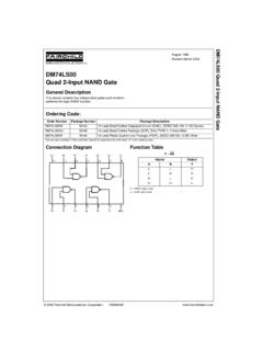
DM74LS00 Quad 2-Input NAND Gate
ecelabs.njit.eduDM74LS00 Quad 2-Input NAND Gate DM74LS00 Quad 2-Input NAND Gate General Description This device contains four independent gates each of which performs the logic NAND function. Ordering Code: Devices also available in Tape and Reel. Specify by appending the suffix letter “X” to the ordering code. Connection Diagram Function Table Y = AB

The basic logic gates arethe inverter (or NOT gate), the ...
www.ee.ic.ac.ukNAND gate, we can build the three basic logic operators: NOT, AND and OR. As a result, we can build ANY logic circuit and implement any Boolean expression. Taken to limit, give me as many NAND gate as I want, in theory I can build a Pentium processor. This shows the universality of the NAND gate. Similarly, one can do the same for NOR gates.
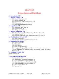
CHAPTER 3 Boolean Algebra and Digital Logic
www2.southeastern.edu3.3.2 Universal Gates 148 Two other common gates are NAND and NOR, which produce complementary output to AND and OR. FIGURE 3.3 and 3.4 The Truth Table and Logic Symbols for NAND and NOR Gates NAND and NOR are known …

EXPERIMENT 3: TTL AND CMOS CHARACTERISTICS
www.classe.cornell.edupossible input combinations to a two-input TTL NAND gate. Figure 3.1 Voltage Level Table for a Two-input TTL NAND Gate. 3.2 You may wonder why the NAND gate is so popular in the TTL logic families. Perhaps the most important factor in the use of …

Data Sheet SAMSUNG PROPRIETARY Samsung V-NAND SSD …
www.samsung.comNAND Flash Memory Samsung V-NAND 3bit MLC DRAM Cache Memory 1GB LPDDR4 2GB LPDDR4 Dimension Max 80.15 x Max 24.15 x Max 8.6 (mm) Form Factor M.2 (2280) Performance (Up to.)2) 3) 4) Sequential Read 7,000 MB/s 7,000 MB/s Sequential Write 5,000 MB/s 5,100 MB/s QD 1 Thread 1 Ran. Read 22K IOPS Ran. Write 60K IOPS 60K IOPS QD 32 …
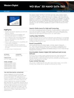
WD Blue 3D NAND SATA SSD - Western Digital
documents.westerndigital.comEvery WD Blue 3D NAND SATA SSD comes with a 5-year limited warranty8, so you can be confident of your storage when you upgrade or replace any of your drives. DATA SHEET INTERNAL DRIVE FOR RETAIL WD Blue™ 3D NAND SATA SSD INTERFACE SATA 6 Gb/s CAPACITIES 250GB to 4TB3 MODEL NUMBERS WDBNCE0040PNC-WRSN …

Quad 2-input NAND gate - Nexperia
assets.nexperia.comQuad 2-input NAND gate Rev. 9 — 22 October 2021 Product data sheet 1. General description The 74HC00; 74HCT00 is a quad 2-input NAND gate. Inputs include clamp diodes. This enables the use of current limiting resistors to interface inputs to voltages in excess of VCC. 2. Features and benefits • Wide supply voltage range from 2.0 to 6.0 V

MC14001B Series B-Suffix Series CMOS Gates
www.farnell.comMC14011B Quad 2−Input NAND Gate MC14023B Triple 3−Input NAND Gate MC14025B Triple 3−Input NOR Gate MC14071B Quad 2−Input OR Gate MARKING DIAGRAMS 1 14 PDIP−14 P SUFFIX CASE 646 MC140xxBCP AWLYYWW SOIC−14 D SUFFIX CASE 751A TSSOP−14 DT SUFFIX CASE 948G 1 14 140xxB AWLYWW 14 0xxB ALYW 1 14
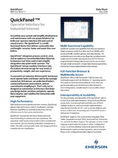
Industrial Internet - Emerson Electric
www.emerson.comQuickPanel+ supports 5 IEC programming languages: Relay Ladder, Sequential Function Chart, Structured Text, Instruction List, and Function Block Diagram. The operator can select multi ... 256MB SLC NAND Flash 512KB Battery Backed SRAM 1GB DDR3 SDRAM 512MB SLC NAND Flash 512KB Battery Backed SRAM Display 6” TFT LCD 320 x 240 Resolution

DM SM2263EN SM2263XT vNF - Silicon Motion
www.siliconmotion.comNAND Flash Channel CE/Channel Max Performance DRAM Interface NAND Flash Support Security Temperature Support Package PCIe Gen3 x4 NVMe 1.3 4 4 Sequential Read: 2,400 MB/s Sequential Write: 1,700 MB/s Random Write: 250K IOPS Supports DDR3, DDR3L, LPDDR3 and DDR4 16-bit data bus width 2 chip enable pins PCIe Gen3 x4 NVMe 1.3 4 4 Sequential …
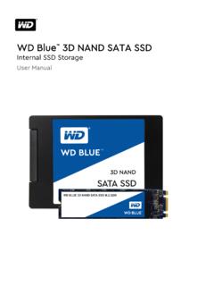
WD Blue 3D NAND SATA SSD - Western Digital
documents.westerndigital.comAvailable in either a SATA 2.5”/7mm cased or an M.2 2280 form factor, the WD Blue 3D NAND SATA SSD offers drive capacities of 250 gigabyte 1 (GB), 500GB, 1 terabyte 2 (TB), and 2TB.

Samsung PM1725b NVMe SSD
image-us.samsung.com3D vertical-NAND (V-NAND) flash memory and an optimized controller. • Outstanding reliability Features three DWPD (drive writes per day) for five years, which equates to 38.4TBs daily, or 7,680 files of 5GB-equivalent data or video every day. • High capacities The 1725b supports a range of capacities, from 1.6TB to an industry leading 15.36TB.
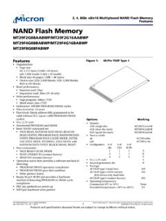
2Gb NAND Flash Memory - Micron Technology
www.micron.com2, 4, 8Gb: x8/x16 Multiplexed NAND Flash Memory List of Figures PDF: 09005aef818a56a7 / Source: 09005aef81590bdd Micron Technology, Inc., reserves the right to change products or specifications without notice.

Experiment 1 - Basic Logic Gates
mems.ece.dal.caExperiment 1 - Basic Logic Gates Objectives: 1. To study the truth tables of various basic logic gates 2. To verify DeMorgan’s Theorem 3. To implement an INVERTER using NAND or NOR gates 4. To implement an OR gate using NAND gates Note: There is no lab report required for this lab. Fill out the observation sheets,

MC14001B - B-Suffix Series CMOS Gates
www.onsemi.comMC14001B Quad 2−Input NOR Gate MC14011B Quad 2−Input NAND Gate MC14023B Triple 3−Input NAND Gate MC14025B Triple 3−Input NOR Gate MC14071B Quad 2−Input OR Gate MARKING DIAGRAMS SOIC−14 D SUFFIX CASE 751A TSSOP−14 DT SUFFIX CASE 948G 1 14 140xxBG AWLYWW 14 0xxB ALYW 1 14 xx = Specific Device Code A = Assembly Location …

eMMC 5.0 Specification compatibility - dzsc.com
file2.dzsc.comeMMC consists of NAND flash and a MMC controller. 3V supply voltage is required for the NAND area (VDDF or VCC) whereas 1.8V or 3V dual supply voltage (VDD or VCCQ) is supported for the MMC controller. SAMSUNG eMMC supports HS400 in order to improve sequential bandwidth, especially sequential read performance.
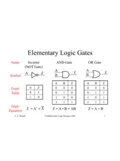
Elementary Logic Gates - Auburn University
eng.auburn.edu• The NAND gate is functionally complete ¾We can build any digital logic circuit out of all NAND gates • Same holds true for the NOR gate and the multiplexer • The XOR & XNOR are not functionally complete Z=AB A B Z=A+B using DeMorgan’s Theorem A B
SPI (Serial Peripheral Interface) NAND Flash Memory
www.endrich.comNAND Flash memory, with specified designed features to ease host management: • User-selectable internal ECC. ECC code is generated internally during a page program operation. When a page is read to the cache register, the ECC code is detect and cor rect the errors when necessary. The 64-bytes spare area is
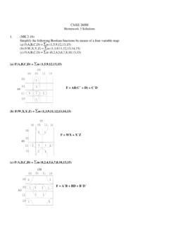
Homework 3 Solutions (c) F(A,B,C,D) = m
www.arl.wustl.edu7. (MK 2-32) Convert the AND/OR/NOT logic diagram in Figure 2-46 to a) a NAND logic diagram and b) a NOR logic diagram a) a NAND logic diagram b) a NOR logic diagram
Samsung PM1725b NVMe SSD
image-us.samsung.comSamsung PM1725b delivers: • Extreme performance The highest level of random read speed and an ultra-low latency rate using Samsung’s highly innovative 3D vertical-NAND (V-NAND) flash memory and an optimized controller. • Outstanding reliability Features three DWPD (drive writes per day) for five years, which equates to 38.4TBs daily, or 7,680
Data Sheet SAMSUNG PROPRIETARY Samsung V-NAND …
semiconductor.samsung.comThe legacy Serial-ATA (SATA) interface faces the theoretical bandwidth limitation of 600MB/s which many SSD manufacturers have tried to reach over the years. Among them, Samsung, which first brought V-NAND technology to the market, continuously strives to improve product reliability and performance, even with the SATA interface limitations.
Lecture Notes for Digital Electronics - University of Oregon
pages.uoregon.eduNote that an INV gate can not be made from OR or AND gates. For this reason the OR and AND gates are not universal. So for example, no combination of AND gates can be combined to substitute for a NOR gate. However, the NAND and NOR gates are universal. 2.2.3 DeMorgan Perhaps the most interesting of the Boolean identities are the two known as ...

Combinational Logic Gates in CMOS
engineering.purdue.edu3-Input NAND gate with Parasitic Capacitors in c out in b in a C p+load C a C b C c P1 P2 P3 R n=0.5R p= C a=C b=C c=C j=0.05pF C p=3C j=0.15pF C load=2C g=0.20pF 2 10 4 1

Rockchip RK3568 Datasheet
www.armdesigner.comJun 01, 2021 · Support Serial NOR Flash, NAND Flash, pSRAM and SRAM Support SDR mode Support 1bit/2bit/4bit data width 1.2.6 System Component CRU (clock & reset unit) Support clock gating control for individual components One oscillator with 24MHz clock input
Gates and Logic: From switches to Transistors, Logic Gates ...
www.cs.cornell.eduLogic Gates • digital circuit that either allows a signal to pass through it or not. • Used to build logic functions • There are seven basic logic gates: AND, OR, NOT, NAND (not AND), NOR (not OR), XOR, and XNOR (not XOR) [later] Building Functions: Logic Gates A B Out 0 0 0 0 1 1 1 0 1 1 1 1 A B Out 0 0 0 0 1 0 1 0 0

Samsung V-NAND SSD 870 QVO - Amazon S3
s3.ap-northeast-2.amazonaws.comMZ-77Q1T0BW MZ-77Q1T0B/AM MZ-77Q1T0B/CN 2TB (2,000GB*) MZ-77Q2T0 Samsung SSD 870 QVO 2TB Warranty Statement MZ-77Q2T0BW MZ-77Q2T0B/AM MZ-77Q2T0B/CN 4TB (4,000GB*) MZ-77Q4T0 Samsung SSD 870 QVO 4TB Warranty Statement MZ-77Q4T0BW MZ-77Q4T0B/AM MZ-77Q4T0B/CN 8TB (8,000GB*) MZ-77Q8T0 Samsung SSD 870 QVO 8TB …

XPG SX6000 Lite PCIe Gen3x4 M.2 2280 Solid State Drive
www.adata.comDec 13, 2018 · XPG SX6000 Lite PCIe Gen3x4 M.2 2280 Solid State Drive Looking to replace your SATA SSD? If so, look no further than the SX6000 Lite PCIe Gen3x4 M.2 2280 SSD. Supporting NVMe 1.3, equipped with 3D NAND Flash, and coming with up to 1TB capacity, the SX6000 Lite is a great upgrade choice. Features Ordering Information

Over-Provisioning Benefits for Samsung Data Center SSDs
semiconductor.samsung.comWith NAND flash, the stored data cannot be overwritten when new data is stored or erased. Since the writing and erasing operations (Program/Erase) of an SSD are carried out in different units, referred to as pages and blocks respectively, multiple cycles of Program and Erase are inevitable in writing and managing data.
Module 5 Logic Diagrams - NTC Sites
sites.ntc.doe.govNOT gate - provides a reversal of the input. If the input is on, the output will be off. If the input is off, the output will be on. Because the NOT gate is frequently used in conjunction with AND and OR gates, special symbols have been developed to represent these combinations. The combination of an AND gate and a NOT gate is called a NAND gate.

Samsung SSD Firmware Update Utility User Manual English
www.samsung.comincorporated into a drive controller. The SATA interface provides functions such as Hot Plugging and NCQ. SSD . Solid State Drive, or SSD, is an innovative data storage device which delivers high performance, reliability, and quality by using NAND Flash memory.

XPG SX6000 Pro PCIe Gen3x4 M.2 2280 Solid State Drive
www.adata.comAug 29, 2018 · XPG SX6000 Pro PCIe Gen3x4 M.2 2280 Solid State Drive Boot, load, and transfer faster with the XPG SX6000 Pro PCIe Gen3x4 M.2 2280 solid state drive (SSD). With support for NVMe 1.3 and equipped with 3D NAND Flash, it offers up to 4 times faster performance than SATA SSDs and up to 1TB of capacity.
Samsung Memory Solutions for Automotive
www.samsung.comautomotive Flash Memory delivers high reliability, extensive product and technical support to keep pace with the long auto production life cycle and a broad portfolio for enhanced customization and compatibility. Samsung's advanced memory solutions for automotive applications NAND Flash Solutions (UFS / eMMC) • Meet AEC-Q100

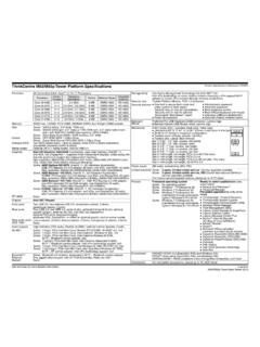
Datasheet - STM32F205xx STM32F207xx - STMicroelectronics
www.st.comperformance from Flash memory, MPU, 150 DMIPS/1.25 DMIPS/MHz (Dhrystone 2.1) Memories – Up to 1 Mbyte of Flash memory – 512 bytes of OTP memory – Up to 128 + 4 Kbytes of SRAM – Flexible static memory controller that supports Compact Flash, SRAM, PSRAM, NOR and NAND memories – LCD parallel interface, 8080/6800 modes

Digital Electronics Lab - brcmcet.edu.in
www.brcmcet.edu.in1. 3 I/P NAND GATE IC 7410 2 2. OR GATE IC 7432 3 3. NOT GATE IC 7404 1 2. IC TRAINER KIT - 1 3. PATCH CORDS - 27 THEORY: ENCODER: An encoder is a digital circuit that performs inverse operation of a decoder. An encoder has 2n input lines and n output lines. In encoder the output lines generates the binary code n

LOGIC GATES (PRACTICE PROBLEMS) - Free GATE ECE 2017 ...
www.gatestudy.comNAND gate satisfies the condition but EX-OR gates does not as it gives 0 output for the same inputs. Option (b) is the correct choice where both gates satisfy the given condition. 3. A locker has been rented in the bank. Express the process of opening the locker in

第1回 デジタル回路の基礎 - 工学院大学
www.ns.kogakuin.ac.jp74LS32 Quad 2-input OR Gates(2入力のORゲート×4) 図9.74LS32のピン配置図(左)と真理値表(右) 本実験で使用するブレッドボードには,74LS00(NAND), 74LS04(NOT), 74LS08(AND), 74LS32(OR), 74LS02(NOR)が図10のように差し込まれている.各ICの1番ピンは,E11, E21, E31, E41, E51に差

Lecture 13 - MIT
web.mit.eduIn practice many gates do not change state every clock cycle which lowers the power dissipation. 6.012 Spring 2007 Lecture 13 14 CMOS Static Logic Gates V OUT V DD V DD A M 1 B M 3 M 4 M 2 M 1 M 2 M 3 M 4 A A B A B (a) (b) B + _ V OUT + _ 6.012 Spring 2007 Lecture 13 15 CMOS NAND Gate I-V Characteristics of n-channel devices V DD V DS1 M 3 4 M ...
ThinkCentre M93/M93p Tower Platform Specifications …
psref.lenovo.comdisk / with 8GB MLC NAND flash memory, SATA 6.0Gb/s Some: ②Solid State Drive (SSD) / SATA 6.0Gb/s, 2.5" Wide Some: DVD-ROM SATA 1.5Gb/s Drive Some: Super Multi-Burner DVD±RW SATA 1.5Gb/s Drive Two SATA cables (each 1-drop to device), three SATA 6.0Gb/s connectors, one eSATA connector (SATA 6.0Gb/s) Optional 29-in-1 media reader, internal …

Integrated Circuit Basics - Electronics
cie-wc.eduDec 20, 2011 · Gate, OR Gate, NAND Gate, NOR Gate and the NOT Gate which is also known as an Inverter. You may also hear about Buffers in future lessons. Pinout Diagrams ... •The next two diagrams are both Quad Two-input NOR Gates. –The difference is that one is a TTL and the other is a CMOS IC. –Look at the difference in the Pinout Diagrams.
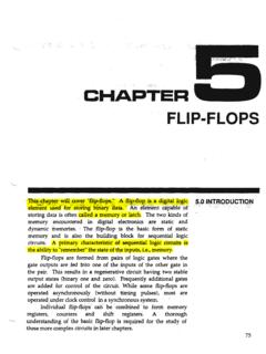
FLIP-FLOPS
www.csun.eduNAND gates to the simple 5-C flip-flop as shown in Figure 5-,.8: Set . a . Clock · a . Clear . Notice that this circuit only provides clock control of the S ...
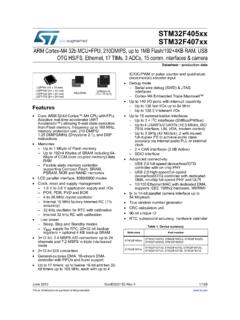
ARM Cortex-M4 32b MCU+FPU, 210DMIPS, up to 1MB …
atta.szlcsc.com– Up to 1 Mbyte of Flash memory – Up to 192+4 Kbytes of SRAM including 64-Kbyte of CCM (core coupled memory) data RAM – Flexible static memory controller supporting Compact Flash, SRAM, PSRAM, NOR and NAND memories • LCD parallel interface, 8080/6800 modes • Clock, reset and supply management – 1.8 V to 3.6 V application supply and I/Os
Flash-based SSDs - University of Wisconsin–Madison
pages.cs.wisc.eduFlash-based SSDs After decades of hard-disk drive dominance, a new form of persistent ... NAND-based flash), which was created by Fujio Masuoka in the 1980s ... Because the process of writing (i.e., erasing and programming) is so un-usual, let’s go through a detailed example to make sure it makes sense. In this example, imagine we have the ...
Similar queries
Digital Phase Locked Loop, 2 2 Input NAND, 2 input, NAND Gate, Input NAND, Input, NAND, 3D NAND, SanDisk, NAND SATA SSD Solid State Drive, SATA, NAND SATA SSD, Gates, Gate, NAND Flash, DRAM, Drive, MC14001B Series B-Suffix Series CMOS, Quad 2, Input NAND gate, Industrial Internet, Programming, Samsung PM1725b NVMe SSD, Flash, Logic gates, NAND gates, EMMC, SAMSUNG eMMC, NAND Flash memory, Homework 3 Solutions, Samsung, Data Sheet SAMSUNG PROPRIETARY, Serial-ATA, Logic: From switches to Transistors, Logic Gates, V-NAND SSD 870 QVO, Solid state drive, SATA SSD, Over-Provisioning, Data, Samsung Memory Solutions for Automotive, Digital Electronics Lab, LOGIC GATES PRACTICE PROBLEMS, Quad