Nand gates
Found 10 free book(s)
Experiment 1 - Basic Logic Gates
mems.ece.dal.caExperiment 1 - Basic Logic Gates Objectives: 1. To study the truth tables of various basic logic gates 2. To verify DeMorgan’s Theorem 3. To implement an INVERTER using NAND or NOR gates 4. To implement an OR gate using NAND gates Note: There is no lab report required for this lab. Fill out the observation sheets,
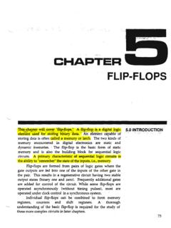
FLIP-FLOPS
www.csun.eduNAND gates to the simple 5-C flip-flop as shown in Figure 5-,.8: Set . a . Clock · a . Clear . Notice that this circuit only provides clock control of the S ...
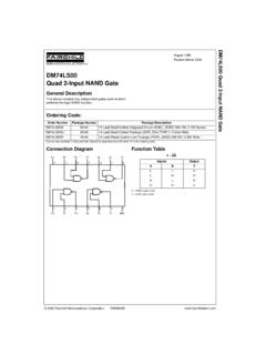
DM74LS00 Quad 2-Input NAND Gate
ecelabs.njit.eduDM74LS00 Quad 2-Input NAND Gate DM74LS00 Quad 2-Input NAND Gate General Description This device contains four independent gates each of which performs the logic NAND function. Ordering Code: Devices also available in Tape and Reel. Specify by appending the suffix letter “X” to the ordering code. Connection Diagram Function Table Y = AB

DESIGNING COMBINATIONAL LOGIC GATES IN CMOS
bwrcs.eecs.berkeley.eduof arbitrary digital gates such as NOR, NAND and XOR. The focus will be on combina-tional logic (or non-regenerative) circuits that have the property that at any point in time, the output of the circuit is related to its current input signals by some Boolean expression (assuming that the transients through the logic gates have settled).

CMOS Technology and Logic Gates - MIT OpenCourseWare
ocw.mit.eduNAND Gate Layout Parallel PMOS Transistors A Output on Metal-1 B (A.B) GND V DD A B (A.B) Contact P-Diffusion (in N-well) N-Diffusion Poly wire connects PMOS & NMOS gates Metal 1-Diffusion Series NMOS Transistors 6.884 – Spring 2005 2/07/2005 L03 – CMOS Technology 19

Combinational Logic Gates in CMOS
engineering.purdue.eduCombinational Logic Gates in CMOS References: Adapted from: Digital Integrated Circuits: A Design ... 4-input NAND Gate In1 In2 In3 In4 V DD GND Out ln2 ln1 ln2 Out ln1 ln4 ln3 ln3 ln4. Standard Cell Layout Methodology VDD VSS Well signals Routing Channel metal1 polysilicon. Two Versions of (a+b).c

Lecture 13 - MIT
web.mit.eduIn practice many gates do not change state every clock cycle which lowers the power dissipation. 6.012 Spring 2007 Lecture 13 14 CMOS Static Logic Gates V OUT V DD V DD A M 1 B M 3 M 4 M 2 M 1 M 2 M 3 M 4 A A B A B (a) (b) B + _ V OUT + _ 6.012 Spring 2007 Lecture 13 15 CMOS NAND Gate I-V Characteristics of n-channel devices V DD V DS1 M 3 4 M ...

MC14001B Series B-Suffix Series CMOS Gates
www.farnell.comMC14011B Quad 2−Input NAND Gate MC14023B Triple 3−Input NAND Gate MC14025B Triple 3−Input NOR Gate MC14071B Quad 2−Input OR Gate MARKING DIAGRAMS 1 14 PDIP−14 P SUFFIX CASE 646 MC140xxBCP AWLYYWW SOIC−14 D SUFFIX CASE 751A TSSOP−14 DT SUFFIX CASE 948G 1 14 140xxB AWLYWW 14 0xxB ALYW 1 14 xx = Specific Device Code A …
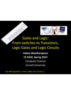
Gates and Logic: From switches to Transistors, Logic Gates ...
www.cs.cornell.eduLogic Gates • digital circuit that either allows a signal to pass through it or not. • Used to build logic functions • There are seven basic logic gates: AND, OR, NOT, NAND (not AND), NOR (not OR), XOR, and XNOR (not XOR) [later] Building Functions: Logic Gates A B Out 0 0 0 0 1 1 1 0 1 1 1 1 A B Out 0 0 0 0 1 0 1 0 0
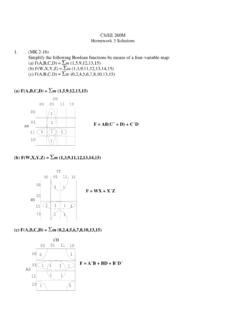
Homework 3 Solutions (c) F(A,B,C,D) = m
www.arl.wustl.eduConvert the AND/OR/NOT logic diagram in Figure 2-46 to a) a NAND logic diagram and b) a NOR logic diagram a) a NAND logic diagram b) a NOR logic diagram 8. When A, B or C changes, the output can change after 3 ns. This is the minimum. Changes in C or D can cause output changes after 6 ns. This is the maximum.