Example: tourism industry
Homework 3 Solutions (c) F(A,B,C,D) = m
7. (MK 2-32) Convert the AND/OR/NOT logic diagram in Figure 2-46 to a) a NAND logic diagram and b) a NOR logic diagram a) a NAND logic diagram b) a NOR logic diagram
Tags:
Information
Domain:
Source:
Link to this page:
Documents from same domain

CSE 473 – Introduction to Computer Networks Jon …
www.arl.wustl.eduCSE 473 – Introduction to Computer Networks Jon Turner Exam 1 Solution 9/26/2013 - 2 - 2. (10 points).

Designing Digital Circuits a modern approach
www.arl.wustl.edu4 Computer-Aided Design 51 ... 9 Still More VHDL 149 9.1 Making Circuit Speci cations More Generic . . . . . . . . . .149 ... Nonetheless, when designing digital circuits we can largely ignore the underlying physics and focus most of our attention on how

How to Write a Great Research Paper
www.arl.wustl.edu3 Start with Good Writing Poorly written papers don’t get read » and are less likely to be published in first place » papers that don’t get read cannot have an impact Write well & others will make a point to read your work » even if they are not working in your area

Designing Digital Circuits a modern approach
www.arl.wustl.edu9.1 Making Circuit Speci cations More Generic . . . . . . . . . .149 ... There are two key inventions that have driven the digital revolution. The rst was the invention of the transistor in the late 1940s, ... of a digital circuit is that it uses voltages and currents to represent logical values, commonly denoted as ‘0’ and ‘1’. Now ...
Related documents

EXPERIMENT 3: TTL AND CMOS CHARACTERISTICS
www.classe.cornell.edupossible input combinations to a two-input TTL NAND gate. Figure 3.1 Voltage Level Table for a Two-input TTL NAND Gate. 3.2 You may wonder why the NAND gate is so popular in the TTL logic families. Perhaps the most important factor in the use of …

Rockchip RK3568 Datasheet
www.armdesigner.comJun 01, 2021 · Support Serial NOR Flash, NAND Flash, pSRAM and SRAM Support SDR mode Support 1bit/2bit/4bit data width 1.2.6 System Component CRU (clock & reset unit) Support clock gating control for individual components One oscillator with 24MHz clock input
CHAPTER 3 Boolean Algebra and Digital Logic
www2.southeastern.edu3.3.2 Universal Gates 148 Two other common gates are NAND and NOR, which produce complementary output to AND and OR. FIGURE 3.3 and 3.4 The Truth Table and Logic Symbols for NAND and NOR Gates NAND and NOR are known …
WD Blue 3D NAND SATA SSD - Western Digital
documents.westerndigital.comAvailable in either a SATA 2.5”/7mm cased or an M.2 2280 form factor, the WD Blue 3D NAND SATA SSD offers drive capacities of 250 gigabyte 1 (GB), 500GB, 1 terabyte 2 (TB), and 2TB.
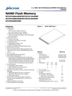
2Gb NAND Flash Memory - Micron Technology
www.micron.com2, 4, 8Gb: x8/x16 Multiplexed NAND Flash Memory List of Figures PDF: 09005aef818a56a7 / Source: 09005aef81590bdd Micron Technology, Inc., reserves the right to change products or specifications without notice.
NAND & NOR Implementation - Digital Logic Design (EEE 241)
digitallogicdesign.weebly.comMultilevel NAND circuits •Multilevel circuits conversion rules: 1.Convert all AND gates to NAND with AND-invert symbols 2.Convert all OR gates to NAND with invert-OR symbols 3.Check all bubbles in diagram. For every bubble that is not compensated by another bubble, insert …
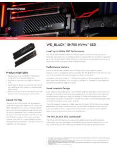
Product Brief: WD Black SN750 NVMe SSD - Western Digital
documents.westerndigital.comWD_BLACK SN750 NVMe SSD (Without Heatsink) Specification Interface M.2 22801,2 PCIe Gen3 8 Gb/s, up to 4 Lanes Formatted Capacity 3 250GB, 500GB, 1TB, 2TB, 4TB Performance² 250GB 500GB 1TB 2TB 4TB Sequential Read up to (MB/s) (Queues=32, Threads=1) 3,100 3,430 3,430 3,400 3,400