Transcription of SP3222E / SP3232E Data Sheet - Exar
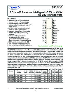
1 True to RS-232 Transceivers SP3222E / SP3232E1/21 REV Meets true EIA/TIA-232-F standards from a to power supply Minimum 120kbps data rate under full load 1 A low power shutdown with receivers active ( SP3222E ) Interoperable with RS-232 down to a power source Enhanced ESD specifications: 15kV Human Body Model 15kV IEC61000-4-2 Air Discharge 8kV IEC61000-4-2 Contact DischargeDescriptionThe SP3222E and SP3232E series are RS-232 transceiver solutions intended for portable or hand-held applications such as notebook or palmtop computers. The SP3222E / SP3232E series has a high-efficiency, charge-pump power supply that requires only F capacitors in operation. This charge pump allows the SP3222E / SP3232E series to deliver true RS-232 performance from a single power supply ranging from to The SP3222E / SP3232E are 2-driver / 2-receiver devices.
2 This series is ideal for portable or hand-held applications such as notebook or palmtop computers. The ESD tolerance of the SP3222E / SP3232E devices are over 15kV for both Human Body Model and IEC61000-4-2 Air discharge test methods. The SP3222E device has a low-power shutdown mode where the devices driver outputs and charge pumps are disabled. During shutdown, the supply current falls to less than 1 ApplicationsOrdering Information - Page 21SP3222E24653719 GNDT1 INT2 INT1 OUTT2 OUTC1+C1-C2+C2-V+ F+C2C5C1++*C3C4++ F 817RS-232 OUTPUTSRS-232 INPUTSLOGICINPUTSVCC1815k R1 INR1 OUT1595k R2 INR2 OUT1016 LOGICOUTPUTSEN20 SHDN*can be returned to either VCC or GNDSSOPTSSOPSP3222E24653717 GNDT1 INT2 INT1 OUTT2 OUTC1+C1-C2+C2-V+ F+C2C5C1++*C3C4++ F815RS-232 OUTPUTSRS-232 INPUTSLOGICINPUTSVCC1615k R1 INR1 OUT1395k R2 INR2 OUT1014 LOGICOUTPUTSEN18 SHDN*can be returned to either VCC or GND SOICSP3232E13542616 GNDT1 INT2 INT1 OUTT2 OUTC1+C1-C2+C2-V+ F+C2C5C1++*C3C4++147RS-232 OUTPUTSRS-232 INPUTSLOGICINPUTSVCC155k R1 INR1 OUT12135k R2 INR2 OUT98 LOGICOUTPUTS*can be returned to
3 Either VCC or FSP3222E / SP3232E2/21 REV Maximum RatingsThese are stress ratings only and functional operation of the device at these ratings or any other above those indicated in the operation sections of the specifications below is not implied. Exposure to absolute maximum rating conditions for extended periods of time may affect reliability and cause permanent damage to the device. to +(1).. to (1).. to + + |V-|(1)..13 VICC (DC VCC or GND current).. 100mAInput VoltagesTxIN, EN, to (VCC + ) 25 VOutput to (VCC + )Electrical CharacteristicsUnless otherwise noted, the following specifications apply for VCC = to with TAMB = TMIN to TMAX, typical values apply at VCC = or and TAMB = 25 CharacteristicsSupply load, VCC = ,TAMB = 25oC, TxIN = GND or VCCS hutdown supply ASHDN = GND, VCC = ,TAMB = 25oC, TxIN = Vcc or GNDL ogic Inputs and Receiver OutputsInput logic threshold , EN, SHDN(2)Input logic threshold = (2)Input logic threshold = (2)
4 Input leakage current+ + ATxIN, EN, SHDN,TAMB = 25oC, VIN = 0V to VCCO utput leakage current+ +10 AReceivers disabled, VOUT = 0V to VCCO utput voltage = voltage HIGHVCC - - = OutputsOutput voltage swing + + driver outputs loaded with 3k to GND, TAMB = 25oCOutput resistance300 VCC = V+ = V- = 0V, TOUT = +2 VOutput short-circuit current+35+60mAVOUT = 0 VOutput leakage current+25 AVCC = 0V or to , VOUT = +12V, drivers disabledShort-Circuit ..-65 C to +150 CPower Dissipation per package20-pin SSOP (derate C above 70 C)..750mW18-pin SOIC (derate C above 70 C)..1260mW20-pin TSSOP (derate C above 70 C)..890mW16-pin SSOP (derate C above 70 C)..775mW16-pin PDIP (derate C above 70 C)..1150mW16-pin WSOIC (derate C above 70 C).
5 900mW16-pin TSSOP (derate C above 70 C)..850mW16-pin NSOIC (derate C above 70 C)..1086mWNOTE:1. V+ and V- can have maximum magnitudes of 7V, but their absolute differ-ence cannot exceed / SP3232E3/21 REV Characteristics (Continued)Unless otherwise noted, the following specifications apply for VCC = to with TAMB = TMIN to TMAX, typical values apply at VCC = or and TAMB = 25 InputsInput voltage range-1515 VInput threshold = threshold = threshold = threshold = resistance357k Timing CharacteristicsMaximum data rate 120235kbpsRL = 3k , CL = 1000pF, one driver switchingDriver propagation delay, sRL = 3k , CL = 1000pFDriver propagation delay, sRL = 3k , CL = 1000pFReceiver propagation delay, sReceiver input to receiver output, CL = 150pFReceiver propagation delay, sReceiver input to receiver output, CL = 150pFReceiver output enable time200nsReceiver output disable time200nsDriver skew100500ns| tPHL - tPLH |.
6 TAMB = 25 CReceiver skew2001000ns| tPHL - tPLH |Transition-region slew rate30V/ sVCC = , RL = 3k , CL = 1000pF, TAMB = 25 C, measurements taken from to or to :2. Driver input hysteresis is typically / SP3232E4/21 REV Performance CharacteristicsUnless otherwise noted, the following performance characteristics apply for VCC = , 120kbps data rate, all drivers loaded with 3k , F charge pump capacitors, and TAMB = 25 1: Transmitter Output Voltage vs Load Capacitance for the SP3222E and SP3232 EFigure 2: Slew Rate vs Load Capacitance for the SP3222E and SP3232 EFigure 3: Supply Current VS. Load Capacitance when Transmitting Data6420-2-4-6 Transmitter Output Voltage [V]Load Capacitance [pF]Vout+Vout-50010001500200001412108642 0 Slew Rate [V/ s ]Load Capacitance [pF]+Slew-Slew05001000150020002330504540 35302520151050 Supply Current [mA]Load Capacitance [pF]118 KHz60 KHz10 KHz05001000150020002330SP3222E / SP3232E5/21 REV FunctionsPin NamePin Function / DescriptionPin NumberSP3222 ESP3232 ESOICSSOPTSSOPENR eceiver Enable.
7 Apply logic LOW for normal logic HIGH to disable the receiver outputs (high-Z state).11-C1+Positive terminal of the voltage doubler charge-pump capacitor221V+ output generated by the charge pump332C1-Negative terminal of the voltage doubler charge-pump capacitor443C2+Positive terminal of the inverting charge-pump capacitor554C2-Negative terminal of the inverting charge-pump output generated by the charge pump776T1 OUTRS-232 driver output151714T2 OUTRS-232 driver output887R1 INRS-232 receiver input141613R2 INRS-232 receiver input998R1 OUTTTL/CMOS receiver output131512R2 OUTTTL/CMOS receiver output10109T1 INTTL/CMOS driver input121311T2 INTTL/CMOS driver to supply voltage171916 SHDNS hutdown Control Input. Drive HIGH for normal device LOW to shutdown the drivers (high-Z output) and the on-board power connect-11, 14-Table 1: Device Pin DescriptionSP3222E / SP3232E6/21 REV +V+C1-C2+ +V+C1-C2+C2-ENR1 INGNDVCCT1 OUT891011R2 INSP3222ET2 OUTT2 INT1 INR1 OUTSOICR2 OUTF igure 4: Pinout Configurations for the SP3222EV-123413141516567121110C1+V+C1-C2 +C2-R1 INR2 INGNDVCCT1 OUTT2IN89SP3232ET1 INR1 OUTR2 OUTT2 OUTF igure 5: Pinout Configurations for the SP3232 ESP3222E / SP3232E7/21 REV Operating CircuitsFigure 6: SP3222E Typical Operating CircuitsFigure 7.
8 SP3232E Typical Operating CircuitSP3222E24653719 GNDT1 INT2 INT1 OUTT2 OUTC1+C1-C2+C2-V+ F+C2C5C1++*C3C4++ F 817RS-232 OUTPUTSRS-232 INPUTSLOGICINPUTSVCC1815k R1 INR1 OUT1595k R2 INR2 OUT1016 LOGICOUTPUTSEN20 SHDN*can be returned to either VCC or GNDSSOPTSSOPSP3222E24653717 GNDT1 INT2 INT1 OUTT2 OUTC1+C1-C2+C2-V+ F+C2C5C1++*C3C4++ F815RS-232 OUTPUTSRS-232 INPUTSLOGICINPUTSVCC1615k R1 INR1 OUT1395k R2 INR2 OUT1014 LOGICOUTPUTSEN18 SHDN*can be returned to either VCC or GND SOICSP3232E13542616 GNDT1 INT2 INT1 OUTT2 OUTC1+C1-C2+C2-V+ F+C2C5C1++*C3C4++147RS-232 OUTPUTSRS-232 INPUTSLOGICINPUTSVCC155k R1 INR1 OUT12135k R2 INR2 OUT98 LOGICOUTPUTS*can be returned to either VCC or FSP3222E / SP3232E8/21 REV InformationThe SP3222E / SP3232E transceivers meet the EIA/TIA-232 and ITU-T communication protocols and can be implemented in battery-powered, portable, or hand-held applications such as notebook or palmtop computers.
9 The SP3222E / SP3232E devices feature MaxLinear s proprietary on-board charge pump circuitry that generates for RS-232 voltage levels from a single to power supply. This series is ideal for systems, mixed to systems, or systems that require true RS-232 performance. The SP3222E / SP3232E devices can operate at a typical data rate of 235kbps when fully SP3222E and SP3232E are 2-driver / 2-receiver devices ideal for portable or hand-held applications. The SP3222E features a 1 A shutdown mode that reduces power consumption and extends battery life in portable systems. Its receivers remain active in shutdown mode, allowing external devices such as modems to be monitored using only 1 A supply of OperationThe SP3222E / SP3232E series is made up of three basic circuit blocks:1.
10 Drivers2. Receivers3. The MaxLinear proprietary charge pumpDriversThe drivers are inverting level transmitters that convert TTL or CMOS logic levels to EIA/TIA-232 levels with an inverted sense relative to the input logic levels. Typically, the RS-232 output voltage swing is with no load and 5V minimum fully loaded. The driver outputs are protected against infinite short-circuits to ground without degradation in reliability. Driver outputs will meet EIA/TIA-562 levels of with supply voltages as low as The drivers can guarantee a data rate of 120kbps fully loaded with 3k in parallel with 1000pF, ensuring compatability with PC-to-PC communication slew rate of the driver is internally limited to a maximum of 30V/ s in order to meet the EIA standards (EIA RS-232D , Paragraph 5).