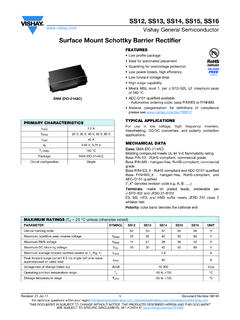
Transcription of Surface-Mount Schottky Barrier Rectifier
1 SS32, SS33, SS34, SS35, General Semiconductor Revision: 23-Apr-20201 Document Number: 88751 For technical questions within your region: DOCUMENT IS SUBJECT TO CHANGE WITHOUT NOTICE. THE PRODUCTS DESCRIBED HEREIN AND THIS DOCUMENTARE SUBJECT TO SPECIFIC DISCLAIMERS, SET FORTH AT Schottky Barrier RectifierLINKS TO ADDITIONAL RESOURCESFEATURES Low profile package Ideal for automated placement Guardring for overvoltage protection Low power losses, high efficiency Low forward voltage drop High surge capability Meets MSL level 1, per J-STD-020, LF maximum peak of 260 C AEC-Q101 qualified available - Automotive ordering code: base P/NHE3 or P/NHM3 Material categorization: for definitions of compliance please see APPLICATIONSFor use in low voltage high frequency inverters, freewheeling, DC/DC converters, and polarity protection DATACase: SMC (DO-214AB) Molding compound meets UL 94 V-0 flammability rating Base P/N-E3 - RoHS-compliant, commercial grade Base P/N-M3 - halogen-free, RoHS-compliant, commercial grade Base P/NHE3_X - RoHS-compliant and AEC-Q101 qualified Base P/NHM3_X - halogen-free, RoHS-compliant, and AEC-Q101 qualified ( _X denotes revision code A, B.)
2 Terminals: matte tin plated leads, solderable per J-STD-002 and JESD 22-B102 E3, M3, HE3, and HM3 suffix meets JESD 201 class 2 whisker testPolarity: color band denotes the cathode endPRIMARY CHARACTERISTICSIF(AV) AVRRM20 V, 30 V, 40 V, 50 V, 60 VIFSM100 AEAS20 V, VTJ CPackageSMC (DO-214AB)Circuit configurationSingleSMC (DO-214AB) CathodeAnodeDesign ToolsRelatedDocuments333 DDD3D3D ModelsModelsApplicationNotesAMarkingAvai lableAvailableMAXIMUM RATINGS (TA = 25 C unless otherwise noted)PARAMETERSYMBOLSS32SS33SS34SS35SS3 6 UNITD evice marking codeS2S3S4S5S6 Maximum repetitive peak reverse voltageVRRM2030405060 VMaximum RMS voltageVRMS1421283542 VMaximum DC blocking voltageVDC2030405060 VMaximum average forward rectified current at TL (fig. 1)IF(AV) forward surge current ms single half sine-wave superimposed on rated loadIFSM100 ANon-repetitive avalanche energy at TA = 25 C, IAS = A, L = 10 mHEAS20mJVoltage rate of change (rated VR)dV/dt10 000V/ sOperating junction temperature rangeTJ -55 to +150 CStorage temperature rangeTSTG-55 to +150 CSS32, SS33, SS34, SS35, General Semiconductor Revision: 23-Apr-20202 Document Number: 88751 For technical questions within your region: DOCUMENT IS SUBJECT TO CHANGE WITHOUT NOTICE.
3 THE PRODUCTS DESCRIBED HEREIN AND THIS DOCUMENTARE SUBJECT TO SPECIFIC DISCLAIMERS, SET FORTH AT (1)Pulse test: 300 s pulse width, 1 % duty cycleNote(1)PCB mounted with " x " (14 mm x 14 mm) copper pad areasNote(1)AEC-Q101 qualifiedRATINGS AND CHARACTERISTICS CURVES (TA = 25 C unless otherwise noted)Fig. 1 - Forward Current Derating CurveFig. 2 - Maximum Non-Repetitive Peak Forward Surge CurrentELECTRICAL CHARACTERISTICS (TA = 25 C unless otherwise noted)PARAMETERTEST CONDITIONSSYMBOLSS32SS33SS34SS35SS36 UNITM aximum instantaneous forward voltage (1) DC reverse current at rated DC blocking voltage (1)TA = 25 = 100 C2010 THERMAL CHARACTERISTICS (TA = 25 C unless otherwise noted)PARAMETERSYMBOLSS32SS33SS34SS35SS3 6 UNITT ypical thermal resistance (1)R JA55 C/WR JL17 ORDERING INFORMATION (Example)PREFERRED P/NUNIT WEIGHT (g)PREFERRED PACKAGE CODEBASE QUANTITYDELIVERY MODESS36-E3 " diameter plastic tape and reelSS36-E3 " diameter plastic tape and reelSS36HE3_B/H (1) " diameter plastic tape and reelSS36HE3_B/I (1) " diameter plastic tape and reelSS36-M3 " diameter plastic tape and reelSS36-M3 " diameter plastic tape and reelSS36HM3_A/H (1) " diameter plastic tape and reelSS36HM3_A/I (1) " diameter plastic tape and reel Forward Rectified Current (A)
4 Lead Temperature ( C)PCB Mounted on " x "(14 mm x 14 mm) Copper Pad AreaSS32 thru SS36110100020406080100 Number of Cycles at 60 HzPeak Forward Surge Current (A)At Rated ms Single Half Sine-WaveSS32, SS33, SS34, SS35, General Semiconductor Revision: 23-Apr-20203 Document Number: 88751 For technical questions within your region: DOCUMENT IS SUBJECT TO CHANGE WITHOUT NOTICE. THE PRODUCTS DESCRIBED HEREIN AND THIS DOCUMENTARE SUBJECT TO SPECIFIC DISCLAIMERS, SET FORTH AT 3 - Typical Instantaneous Forward CharacteristicsFig. 4 - Typical Reverse Current CharacteristicsFig. 5 - Typical Junction CapacitanceFig. 6 - Typical Transient Thermal ImpedancePACKAGE OUTLINE DIMENSIONS in inches (millimeters) lineInstantaneous Forward Current (A)Instantaneous Forward Voltage (V)TJ=150 CTJ=-40 CTJ=25 line2nd lineInstantaneous Reverse Current (mA)Percent of Rated Peak Reverse Voltage (%)TJ=125 CTJ=75 CTJ=-40 CTJ=25 CTJ= 150 Voltage (V)Junction Capacitance (pF)100SS32 thru SS34SS35 and SS36TJ = 25 Cf = MHzVsig = 50 Thermal Impedance ( C/W)t - Pulse Duration (s)Cathode BandSMC (DO-214AB) ( ) ( ) ( ) ( ) ( ) ( ) ( ) ( ) ( )0 (0) ( ) ( ) ( ) ( ) ( ) ( )Mounting Pad ( ) ( ) ( ) ( ) Disclaimer Revision: 09-Jul-20211 Document Number: 91000 Disclaimer ALL PRODUCT, PRODUCT SPECIFICATIONS AND DATA ARE SUBJECT TO CHANGE WITHOUT NOTICE TO IMPROVE RELIABILITY, FUNCTION OR DESIGN OR OTHERWISE.
5 Vishay Intertechnology, Inc., its affiliates, agents, and employees, and all persons acting on its or their behalf (collectively, Vishay ), disclaim any and all liability for any errors, inaccuracies or incompleteness contained in any datasheet or in any other disclosure relating to any makes no warranty, representation or guarantee regarding the suitability of the products for any particular purpose or the continuing production of any product. To the maximum extent permitted by applicable law, Vishay disclaims (i) any and all liability arising out of the application or use of any product, (ii) any and all liability, including without limitation special, consequential or incidental damages, and (iii) any and all implied warranties, including warranties of fitness for particular purpose, non-infringement and regarding the suitability of products for certain types of applications are based on Vishay's knowledge of typical requirements that are often placed on Vishay products in generic applications.
6 Such statements are not binding statements about the suitability of products for a particular application. It is the customer's responsibility to validate that a particular product with the properties described in the product specification is suitable for use in a particular application. Parameters provided in datasheets and / or specifications may vary in different applications and performance may vary over time. All operating parameters, including typical parameters, must be validated for each customer application by the customer's technical experts. Product specifications do not expand or otherwise modify Vishay's terms and conditions of purchase, including but not limited to the warranty expressed included in this datasheet may direct users to third-party websites. These links are provided as a convenience and for informational purposes only. Inclusion of these hyperlinks does not constitute an endorsement or an approval by Vishay of any of the products, services or opinions of the corporation, organization or individual associated with the third-party website.
7 Vishay disclaims any and all liability and bears no responsibility for the accuracy, legality or content of the third-party website or for that of subsequent as expressly indicated in writing, Vishay products are not designed for use in medical, life-saving, or life-sustaining applications or for any other application in which the failure of the Vishay product could result in personal injury or death. Customers using or selling Vishay products not expressly indicated for use in such applications do so at their own risk. Please contact authorized Vishay personnel to obtain written terms and conditions regarding products designed for such license, express or implied, by estoppel or otherwise, to any intellectual property rights is granted by this document or by any conduct of Vishay. Product names and markings noted herein may be trademarks of their respective owners. 2021 VISHAY INTERTECHNOLOGY, INC.
8 ALL RIGHTS RESERVED