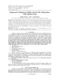
Transcription of Technical Note VXIbus Overview - vxitech.com
1 140 Online at 955 1894 Prior to 1987 there existed only one major architecturestandard for General Purpose Interface Bus(GPIB). Although the GPIB was widely used, it did not addressthe need for portable test stations, nor for the market demandfor faster, more cost-effective test solutions. In 1987, aconsortium of test and measurement companies new standard instrument architecture. The VXIbus (VMEbus eXtensions for Instrumentation) was developed tomeet the need for portable applications and to provide astandard modular open architecture for integrating into thetraditional GPIB test system and for stand-alone was designed to be an open architecture standard forinstruments on a card, allowing an instrument from anymanufacturer to operate in the same mainframe as anothermanufacturer's than design an entirely new architecture, the VXIbusConsortium decided to enhance an existing standard that waswell accepted in the data acquisition and high-speed VMEbus architecture, known for its excellent computerbackplane, high-speed data rates of 40 MB/s, along with thenecessary communication protocols, made it ideal for buildinginstrument systems for high throughputs.
2 VXIbusincorporates the ease-of-use features of intelligent GPIB instruments (for example, ASCII-level programming) into itsmessage-based device, and also takes advantage of the highthroughput capability of VME devices, which are programmedand communicate directly in binary (register-based devices).Although VME is an excellent computer backplane, it is notadequate for instrumentation without further VXIbus Consortium enhanced the VMEbus standard byfurther defining parameters to allow users to easily configurea workable system. Some of the enhancements added to theVMEbus standard were: Larger card options for higher performance instruments and to add shielding. Defining all signals on the backplane, avoiding problems due to user-defined signals on the VMEbus. Addition of EMC, cooling and power specifications to further ease system integration.
3 Definition of communication protocols to ease integration with existing test systems. Addition of voltages for high-performance VXIbus system or subsystem consists of a VXIbusmainframe, VXIbus devices, a VXIbus slot 0 card, VXIbusresource manager, and host controller. The slot 0 takes careof backplane management and includes things such as clocksources and arbitration for data movement across thebackplane. The module that goes into this slot must performthese hardware functions in addition to its normal resource manager configures the modules for properoperation whenever the system is powered on or reset,allowing the user to build the test system software from aknown starting point. The resource manager is not involvedwith the VXIbus system once normal operation begins. TheVXIbus mainframe houses the VXIbus instruments andcontains the power and cooling mechanism for theseinstruments, as well as the communication VXIbus was not designed to replace any existingstandard, but instead as an additional tool to help in overalltest or data acquisition solutions.
4 To this end several methodsof communicating with VXIbus devices were defined, enablingVXIbus solutions to be integrated with VMEbus, GPIB or asstand-alone portable solutions. MECHANICALThe VXIbus specification defines four module sizes. The twosmaller sizes, A and B, are the defined VMEbus module sizesand are true VMEbus modules in every sense. The two largersizes, C and D, are for higher performance module spacing in the C- and D-size systems makesit possible to fully shield sensitive circuits for highperformance C-size VXIbus footprint has become the most commonsize today because it keeps systems to a smaller size than D,and allows the performance of VXIbus to be utilized (A and Bbeing VMEbus devices). The only real D-size solutions foundtoday are in large functional testers that include instrumentsor custom circuits that were developed on D-size because ofreal estate advantages.
5 B-size solutions are available, butconsist mainly of VMEbus type or low-performanceinstruments, and do not utilize the benefits of the VXIbusstandard. Ninety percent of VXIbus products on the currentmarket conform to the C-size footprint. ELECTRICALA dditional power supply voltages for powering analog andECL circuits and instrumentation buses for measurementsynchronization and triggering were added to the existingVMEbus signal, along with an analog sum-bus and a set oflocal bus lines for private module-to-module communication. Technical NoteTechnical NoteVXIbus Overview Specification OverviewVXIbus BasicsIntroduction141 Online at 955 1894 Figure 1D Size2 cm( in.)3 cm( in.)3 cm( in.)3 cm( in.)10 x 16 cm( x in.) x 16 cm( x in.) x 34 cm( x in.) x 34 cm( x in.)Card SizeCard SpacingA SizeB SizeC SizeThe VXIbus specifies three 96-pin DIN connectors called P1,P2, and P3.
6 The P1 connector, the only mandatory one in VMEor VXIbus , carries the data transfer bus (up to 24 bitsaddressing and 16 bits data), the interrupt bus, and optional P2 connector, available to all card sizes except A-size, expands the data transfer bus to its full 32-bit size. It alsoadds four additional power supply voltages, the local bus, themodule identification bus (allows a VXIbus module's slotnumber to be determined), and the analog summing bus (acurrent summing bus that runs the length of the backplane).Also, there are TTL and ECL trigger buses (running the lengthof the backplane with four trigger protocols defined) and a 10 MHz differential ECL clock signal (buffered to each slot).P3 The optional P3 connector, available only on D-size, expandsP2 resources for specialized applications. It provides 24 morelocal bus lines, additional ECL trigger lines, and 100 MHz clockand star trigger lines for precision OverviewTechnical NoteTechnical NoteLocal BusThe local bus adds significant capability to VXIbusmeasurement systems.
7 It is a very flexible daisy-chain busstructure. Every inner slot in a VXIbus mainframe has a setof very short, 50 ohm transmission lines running betweenadjacent slots on either side. The local bus is 12 lines wideeach direction through the P2 connector and an additional 24lines wide through the P3 connector. This bus allows foradjacent modules to perform private 1 shows the actual pin outs of P1 and P2 for has not been shown, because of lack of use, but can befound in the VXIbus VXIbus specification stipulates radiated and conductedEMC limits for both generation and susceptibility. Theimportance of this part of the VXIbus specification cannot beoverstated. EMC limits ensure that modules containingsensitive electronic circuits perform to expectations withoutinterference from any other module operating in the AND COOLINGIn a typical IEEE-488 rack-and-stack or VMEbus system, thesystem integrator must take a rigorous approach to ensurean environment cool enough for proper operation.
8 Eachinstrument's power dissipation, airflow and placement in therack must be considered. The rack's cooling capability mustbe factored in as ensure adequate cooling in a VXIbus system, the designprocess is simpler. Every vendor's mainframe specificationsheet provides a cooling graph for the worst-case moduleconfiguration. It is specified in terms of pressure across themodule versus the airflow delivered. Each instrumentationmanufacturer must also specify the airflow and back pressurerequired by the instrument for proper operation (normally fora 10 C rise in temperature). The user would then plot thepoint of the module's airflow and back pressurespecifications on the mainframe's cooling curve and, iflocated within the boundaries of the curve, the module isguaranteed to be compatible with the power specification is another way the VXIbus makes thesystem integrator's job easier.
9 Each VXIbus mainframe isspecified for power delivered. Each power supply level has apeak DC current delivery and peak-to-peak dynamic currentdelivery. When selecting modules, voltage levels and currentrequirements are compared to the mainframe's VXIbus dynamic current specification ensures that theselected modules will not induce more ripple noise on themainframe's power supply lines than any module is requiredto withstand. (Figure 2)142 Online at 955 1894independent, , Windows, DOS, UNIX. If an externalcomputer is used, the interface to the VXIbus mainframe canalso be flexible, , GPIB/VXI, MXI/VXI, RS-232/VXI,Ethernet/VXI. Any approach used has its own set ofadvantages and disadvantages dependent upon the overallsystem requirements. Each VXIbus mainframe must have aslot 0 card. Because of available real estate, the slot 0functions are typically integrated with the interface to theexternal controller or with the embedded is one unique logical address (ULA) per VXIbus device(numbered from 0 to 255) and up to 256 devices in a VXIbussystem.
10 Typically a voltmeter, switch, or signal generator is asingle device. It is important, however, to understand thatULAs or VXIbus instruments have no relationship to individualVXIbus card slots. The VXIbus specification allows for severaldevices per card slot for improved portability and integration,or one instrument per several card slots for densely modules must have registers located atspecific addresses, as shown in Figure 3. The upper 16kB ofthe 64kB A16 address space are reserved for VXIbus devices. The two most common types of VXIbus devices are registerand message-based. A comparison is shown *BCLR*5D02 ACFAIL*6D03BG0IN*7D04BG0 OUT*D158D05BG1IN*GND9D06BG1 OUT*BG2IN*BG2 OUT*BG3IN*BG3 OUT*SYSFAIL*10D07D08D09D10D11D12D13D14 BERR*11 GNDBR0*SYSRESET*12 SYSCLKBR1*LWORD13 GNDBR2*AM514DS1*BR3*A2315 DSO*AM0A2216 WRITE*AM1A2117 GNDDTACK*GNDGNDAS*AM2A2018 IACK*AM3A1919 IACKIN*GND20 IACKOUT*SERCLK(1)21AM4 SERDAT*(1)22A07 GND23A06 IRQ7*24A05 IRQ6*IRQ5*IRQ4*IRQ3*IRQ2*IRQ1*+5 VSTDBY+5V+5V25A0426A0327A0228A01A15A16A1 7A18A14A13A12A11A10A09A0829-12V+12V30+5V 3132 Row ASignalRow BSignalRow CSignalPinNumberVXIbus P1 Pin Definitions: Slot 0-12 Row ASignalRow BSignalRow CSignal123 ECLTRG0 ECLTRG14-2V+ + + *TTLTRG2*TTLTRG5*TTLTRG7*TTLTRG4*TTLTRG6 *GND22D2423+5VD2524D26D27D28D29D30D31 GND+5V-24V2526 GND27 RSV228 MODID0029 GND+24V30 SUMBUS3132 PinNumberVXIbus P2 Pin Definitions.