Transcription of UV SMD LED PLCC-2 - Vishay Intertechnology
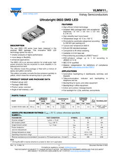
1 Semiconductors Rev. , 26-Jun-171 Document Number: 82556 For technical questions, contact: DOCUMENT IS SUBJECT TO CHANGE WITHOUT NOTICE. THE PRODUCTS DESCRIBED HEREIN AND THIS DOCUMENTARE SUBJECT TO SPECIFIC DISCLAIMERS, SET FORTH AT SMD LED PLCC-2 DESCRIPTIONThe package of the VLMU3100 series is the PLCC-2 . It consists of a lead frame which is embedded in a white thermoplast. The reflector inside this package is filled up with clear silicone which guarantees long life time. The viewing angle is 120 , package dimensions are mm x mm x GROUP AND PACKAGE DATA Product group: LED Package: SMD PLCC-2 Product series: standard Angle of half intensity: 60 Lead-finishing: AgFEATURES UV SMD LED with exceptional brightness High efficient InGaN technology Long life time due to silicone casting Compatible with automatic placement equipment EIA and ICE standard package Compatible with IR reflow and vapor phase Available in 8 mm tape Low profile package Non-diffused lens.
2 Excellent for coupling to light pipes and backlighting Low power consumption Preconditioning according to JEDEC level 2a ESD-withstand voltage: up to 1 kV according to JESD22-A114-B Material categorization: for definitions of compliance please see Curing of glue and laquer Recognition of safety features of money billsSAFETY ADVICESD epending on the mode of operation, these devices emit highly concentrated non visible ultraviolet light which can be hazardous to the human eye. Products which incorporate these devices have to follow the safety precautions given in IEC 60825-1 Safety of Laser Products.
3 19225 PARTS TABLEPARTCOLORRADIANT INTENSITY (mW/sr)at IF(mA)WAVELENGTH(nm)at IF(mA)FORWARD VOLTAGE(V)at IF(mA) MAXIMUM RATINGS (Tamb = 25 C, unless otherwise specified) VLMU3100 PARAMETERTEST CONDITIONSYMBOLVALUEUNITF orward currentIF30mASurge forward currenttp 10 dissipationPtot120mWJunction temperatureTj+100 COperating temperature rangeTamb-40 to +80 CStorage temperature rangeTstg-40 to +100 CSolder temperatureTsol260/5 Semiconductors Rev. , 26-Jun-172 Document Number: 82556 For technical questions, contact: DOCUMENT IS SUBJECT TO CHANGE WITHOUT NOTICE. THE PRODUCTS DESCRIBED HEREIN AND THIS DOCUMENTARE SUBJECT TO SPECIFIC DISCLAIMERS, SET FORTH AT CHARACTERISTICS (Tamb = 25 C, unless otherwise specified)Fig.
4 1 - Forward Current vs. Ambient TemperatureFig. 2 - Forward Current vs. Forward VoltageFig. 3 - Relative Luminous Intensity vs. Angular DisplacementFig. 4 - Relative Intensity vs. WavelengthOPTICAL AND ELECTRICAL CHARACTERISTICS (Tamb = 25 C, unless otherwise specified) VLMU3100, ULTRAVIOLETPARAMETERTEST intensityIF = 20 powerIF = 20 mA wavelengthIF = 20 mA p400405410nmAngle of half intensityIF = 20 mA - 60- degForward voltageIF = 20 currentVR = 5 VIR--10 A051015202530350 102030405060708090100 Tamb - Ambient Temperature ( C)IF - Forward Current (mA)0102030405060100012345VF - Forward Voltage (V)IF - Forward Current (mA) 30 10 20 40 50 60 70 80 rel - Relative Luminous Intensity - Angular Displacement020406080100375400425450475 - Wavelength (nm)Irel - Relative Intensity (%) Semiconductors Rev.
5 , 26-Jun-173 Document Number: 82556 For technical questions, contact: DOCUMENT IS SUBJECT TO CHANGE WITHOUT NOTICE. THE PRODUCTS DESCRIBED HEREIN AND THIS DOCUMENTARE SUBJECT TO SPECIFIC DISCLAIMERS, SET FORTH AT 5 - Specific Luminous Intensity vs. Forward CurrentFig. 6 - Relative Radiant Intensity vs. Ambient TemperaturePACKAGE DIMENSIONS in millimetersSOLDER PAD - Forward Current (mA)Relative Luminous Intensity(Tamb = 25 C) - Ambient Temperature ( C)Ie rel - Relative Radiant Semiconductors Rev. , 26-Jun-174 Document Number: 82556 For technical questions, contact: DOCUMENT IS SUBJECT TO CHANGE WITHOUT NOTICE. THE PRODUCTS DESCRIBED HEREIN AND THIS DOCUMENTARE SUBJECT TO SPECIFIC DISCLAIMERS, SET FORTH AT OF TAPING/POLARITY AND TAPE AND REELSMD LED (VLM3 - SERIES) Vishay s LEDs in SMD packages are available in an antistatic 8 mm blister tape (in accordance with DIN IEC 40 (CO 564) for automatic component insertation.)
6 The blister tape is a plastic strip with impressed component cavities, covered by a top OF TAPEFEEDING DIRECTIONDIMENSIONS OF REEL in millimetersSOLDERING PROFILEFig. 7 - Vishay Lead (Pb)-Free Reflow Soldering Profile(according to J-STD-020C)05010015020025030005010015020 0250300 Time (s)Temperature ( C)240 C245 Cmax. 260 Cmax. 120 smax. 100 s217 Cmax. 30 smax. ramp up 3 C/smax. ramp down 6 C/s19885IR Reflow Soldering Profile for Lead (Pb)-Free SolderingPreconditioning according to JEDEC level 2amax. 2 cycles allowed255 Semiconductors Rev. , 26-Jun-175 Document Number: 82556 For technical questions, contact: DOCUMENT IS SUBJECT TO CHANGE WITHOUT NOTICE.
7 THE PRODUCTS DESCRIBED HEREIN AND THIS DOCUMENTARE SUBJECT TO SPECIFIC DISCLAIMERS, SET FORTH AT CODE PRODUCT LABEL (example only)A. 2D barcodeB. Vishay part numberC. Quantity D. SEL = selection code (binning)E. Code of manufacturing plantF. Batch = date code: year / week / plant codeG. Region codeH. SL = sales locationI. Terminations finishingK. Lead (Pb)-free symbolL. Halogen-free symbolM. RoHS symbolDRY PACKINGThe reel is packed in an anti-humidity bag to protect the devices from absorbing moisture during transportation and PACKINGThe sealed reel is packed into a cardboard box. A secondary cardboard box is used for shipping METHOD OF STORAGEDry box storage is recommended as soon as the aluminum bag has been opened to prevent moisture absorption.
8 The following conditions should be observed, if dry boxes are not available: Storage temperature 10 C to 30 C Storage humidity 60 % RH more than 672 h under these conditions moisture content will be too high for reflow case of moisture absorption, the devices will recover to the former condition by drying under the following condition:192 h at 40 C + 5 C / - 0 C and < 5 % RH (dry air / nitrogen) or 96 h at 60 C + 5 C and < 5 % RH for all device containers or 24 h at 100 C + 5 C not suitable for reel or EIA JEDEC standard JESD22-A112 level 2a label is included on all dry of JESD22-A112 level 2a labelESD PRECAUTIONP roper storage and handling procedures should be followed to prevent ESD damage to the devices especially when they are removed from the antistatic shielding bag.
9 Electro-static sensitive devices warning labels are on the SEMICONDUCTORS STANDARD BAR CODE LABELSThe Vishay Semiconductors standard bar code labels are printed at final packing areas. The labels are on each packing unit and contain Vishay Semiconductors specific bagLabelReel15973 L E V E L CAUTION This bag contains MOISTURE SENSITIVE DEVICES 1. Shelf life in sealed bag 12 months at <40 C and < 90% relative humidity (RH) 2.
10 After this bag is opened devices that will be subjected to infrared reflow, vapor-phase reflow, or equivalent processing (peak package body temp. 260 C) must be: a) Mounted within 672 hours at factory condition of < 30 C/60%RH or b) Stored at <10% RH. 3. Devices require baking before mounting if: a) Humidity Indicator Card is >10% when read at 23 C + 5 C or b) 2a or 2b is not met. 4. If baking is required, devices may be baked for: 192 hours at 40 C + 5 C/-0 C and <5%RH (dry air/nitrogen) or 96 hours at 60 5oCand <5%RH For all device containers or 24 hours at 100 5 C Not suitable for reels or tubes Bag Seal Date: _____ (If blank, see bar code label) Note: LEVEL defined by EIA JEDEC Standard JESD22-A113 2a 19786 Legal Disclaimer Revision: 08-Feb-171 Document Number: 91000 Disclaimer ALL PRODUCT, PRODUCT SPECIFICATIONS AND DATA ARE SUBJECT TO CHANGE WITHOUT NOTICE TO IMPROVE RELIABILITY, FUNCTION OR DESIGN OR OTHERWISE.