Solder
Found 10 free book(s)
HAND SOLDERING TRAINING COURSE - Almit
www.almit.com4 • Formation of a “metal to metal” joint using solder. • The joint is made by alloy formation of base metal and solder. • In soldering, there are three key elements :
KOKI S3X58-M406-3 Lead Free Solder Paste - ADTOOL
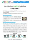
www.adtool.caAnti-Pillow Defect Lead Free Solder Paste S3X48-M406-3 PREVENTS the occurrence of HIDDEN PILLOW DEFECT and ensures the quality of solder joints. Ensures OUTSTANDING continual PRINTABILITY with super fine pitch and CSP applications and has long stencil idle time. Heat RESISTANT new flux formula achieves complete solder melting and wetting on micro-components …
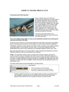
CRIMP VS. SOLDER: PROS & CONS - Davis RF
www.davisrf.comPREFERRED 1. Solder around joint is smooth and shiny 2. No evidence of solder flow outside joint region • Soldering is much more tolerant of non-optimum technique.
Through Hole Solder Joint Evaluation - IPC
www.ipctraining.org3 Through Hole Solder Joint Evaluation Training and Reference Guide Terminology Terminology Solder Destination Side: The side of a through hole assem-bly containing the most com-
NanoStar & NanoFree 300 m Solder Bump Wafer Chip-Scale ...
www.ti.comSBVA017 NanoStar & NanoFree 300 m Solder Bump Wafer Chip-Scale Package Application 5 2 Physical Description 2.1 Package Characteristics The NanoStar package family is a Die Size BGA as identified by the JEDEC standards organiza-

'Evaluation of Nickel/Palladium-Finished ICs With Lead ...
www.ti.comSZZA024 Evaluation of Nickel/Palladium-Finished ICs With Lead-Free Solder Alloys 5 Sn/Pb/Ag solder alloy was the control paste. The Sn/Ag/Cu alloy was chosen because this alloy

ASSOCIATION CONNECTING ELECTRONICS INDUSTRIES …
www.ipc.orgGuide to Solder Paste Assessment 1 SCOPE This handbook is a companion to the solder paste standard J-STD-005 and should be considered to be a guide to help
Dye and Pry of BGA Solder Joints - Cascade Engineering
www.cascade-eng.comDRAM Failure Investigation Equipment Used • Dye and Pry Technique Conclusions • Interfacial fracture / cracks observed at two locations: Solder-CU-PCB Interface
ELECTRONICS INDUSTRIES Qualification and Performance ...
www.ipc.orgQualification and Performance Specification of Permanent Solder Mask 1 SCOPE AND DESIGNATION 1.1 Scope This specification shall define the criteria for and method of obtaining the maximum information about
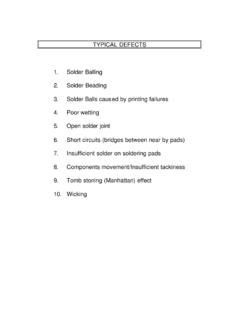
SOLDER PASTE TRAINING - mectronics.in
www.mectronics.in3. SOLDER BALLS CAUSED BY PRINTING FAILURES Solder paste is forced onto non-wettable surfaces such as the solder Mask. Possible reasons: Bad seal between the stencil and the PCB
Similar queries
HAND SOLDERING TRAINING COURSE, Solder, M406-3 Lead Free Solder Paste, CRIMP VS. SOLDER: PROS & CONS, Through Hole Solder Joint Evaluation, NanoStar & NanoFree, Guide to Solder Paste Assessment, And Pry of BGA Solder Joints, Qualification and Performance Specification of Permanent Solder, SOLDER PASTE TRAINING