Chapter 1 Quantum Computing Basics and Concepts
community is mainly due to the Moore’s law [Moo65]; that is: the number of transis-tors in a chip doubles every 18 months and the size of gates is constantly shrinking. Consequently problems such as heat dissipation and information loss are becoming very important for current and future technologies. Improving the scale of transis-
Download Chapter 1 Quantum Computing Basics and Concepts

Information
Domain:
Source:
Link to this page:
Documents from same domain

JEDEC STANDARD - Creating Web Pages in your …
web.cecs.pdx.eduJEDEC STANDARD Preconditioning of Nonhermetic Surface Mount Devices Prior to Reliability Testing JESD22-A113D (Revision of JESD22-A113C) AUGUST 2003

JEDEC PUBLICATION - Creating Web Pages in your …
web.cecs.pdx.eduJEDEC PUBLICATION Failure Mechanisms and Models for Semiconductor Devices JEP122E (Revision of JEP122D, October 2008) Originaly published as JEP122D.01
Zo:Transmission Lines, Reflections, and Termination
web.cecs.pdx.eduTransmission Lines, Reflections, and TerminationZo–1 Supplementary material to accompany Digital Design Principles and Practices, Fourth Edition, by John F. Wakerly. ISBN 0-13-186389-4. 2006 Pearson Education, Inc.,UpperSaddle River, NJ.

Real-time doors and windows recognition in …
web.cecs.pdx.eduReal-time doors and windows recognition in OpenCV using SURF for a guiding ROBOT 1 . Object recognition– in. computer vision, this is the task of …

SAMPLE CALCULATIONS: Chlorine Feed Rate
web.cecs.pdx.eduSAMPLE CALCULATIONS: Chlorine Feed Rate Chlorine is added to water to kill any disease-causing organisms which may be present in the water or may enter the water as it travels through the distribution system.

Controlling Robobuilder Humanoid robot using …
web.cecs.pdx.eduControlling Robobuilder using L# Phil Page 1 06/04/2010 Controlling Robobuilder Humanoid robot using Lisp/L# If you want to give a gripper for your robobuilder, order it now from my Shapeways shop at
A Statistical Distribution Function of Wide …
web.cecs.pdx.eduA Statistical Distribution Function of Wide Applicability By WALODDI WEIBULL,l STOCKHOLM, SWEDEN This paper discusses the applicability of statistics to a
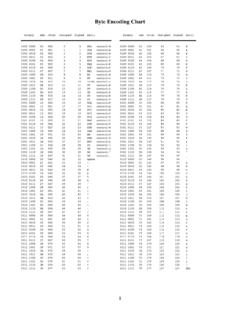
Byte Encoding Chart - Computer Action Team
web.cecs.pdx.eduByte Encoding Chart 2 Binary Hex Octal Unsigned Signed Mac-Courier-Font 1000 0000 80 200 128 -128 Ä 1000 0001 81 201 129 -127 Å
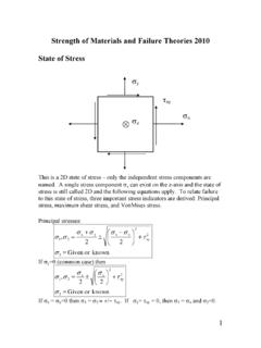
Strength of Materials and Failure Theories
web.cecs.pdx.edu1 Strength of Materials and Failure Theories 2010 State of Stress This is a 2D state of stress – only the independent stress components are
The FPGA Implementation Of Kalma2 - Computer …
web.cecs.pdx.eduThe FPGA Implementation Of Kalman Filter GANG CHEN and LI GUO Department of Electronic Science and Technology University of Science & Technology of China
Related documents

Introduction to Integrated Circuit Technology
www.icknowledge.comDiodes and transis-tors are made with semiconductor material and resistors and capacitors may be made on or in semiconductor materials as well. As the scientific community began to understand semiconductor materials, the transistor and later the IC were invented (see “His-

DIFFERENCES BETWEEN PNP AND NPN
www.tecnical.catThe difference between the two is marked by the design of its internal circuit and the type of transis-tor used. The selection of a PNP sensor relative to an NPN sensor is determined by the nature of the circuit the device is to be used in. When used in a traditional relay type control circuit, it is normally possible to

14. Transistor Characteristics Lab
www.hunter.cuny.eduand what results is a npn transistor. Two laboratory diodes wired back-to-back will NOT make a transis-tor. In a real transistor, the region of the two p regions is very narrow or thin so that the carriers can diffuse across the region freely. The symbol for the npn transistor is Bipolar transistors have three terminals: base, emitter, and ...

Montages à plusieurs transistors - Le Mans University
ressources.univ-lemans.frCe montage est constitué par l’association de deux transis-tors T1 et T2 de même type (deux PNP ou deux NPN). T2 est un transistor de puissance donc de gain en courant petit et dont l’impédance d’entrée h’11 pour le courant nominal est faible ; T1 est un transistor d’usage général de gain normal.

chapter5.fm Page 144 Monday, September 6, 1999 11:41 AM
bwrcs.eecs.berkeley.edu• The logic levels are not dependent upon the relative device sizes, so that the transis-tors can be minimum size. Gates with this property are called ratioless. This is in contrast with ratioed logic, where logic levels are determined by the relative dimen-sions of the composing transistors.

Photodiode/Phototransistor Application Circuit - PhysLab
physlab.orgThe circuit of Figure 4 (B) has an additional transis-tor (Tr2) to provide a larger output current. Cj = AV()D – VR 1 n – ---Figure 3. Photocurrent Amplifier Circuit using Transistor IP OP1-18 RBE VCC Tr1 RL Tr1 RBE VOUT VBE VBE L VCC VOUT IP (A) (B) Figure 4. Photocurrent Amplifier Circuit with Negative Feedback Tr1 R1 R3 VCC R2 VOUT Tr2 ...

5 MOS Field-Effect Transistors (MOSFETs)
learninglink.oup.comFor the circuit in Fig. 5.10.1, the NMOS transis-tor has Vtn = 0.5V, kn = 10mA/V2,andλn = 0, and the PMOS transistor has Vtp =−0.5V, kp = 12.5mA/V2,and|λp|=0. ObservethatQ1 andits surrounding circuit is the same as the circuit ana-lyzedinProblem5.9(Fig.5.9.1),andyoumayuse the results found in the solution to that problem here.

KENWOOD
www.kenwood.comyou even apply power. Note that the final power transis- tors might be damaged during transmission if the trans- ceiver is operated into an improper load. 1. If the built-in antenna tuner is used, operate at full power only after automatic tuning is completed 2. Use only a resonant 50 ohm antenna which has been adjusted for an SWR of 1.5 to 1 ...

Class-E RF Power Amplifiers - Australian National University
people.physics.anu.edu.auceptual “target” waveforms of transis-tor voltage and current that meet the high-efficiency requirements. The tran-sistor is operated as a switch. The volt-age-current product is low throughout the RF period because: 1. “On” state: The voltage is nearly zero when high current is flowing, that is, the transistor acts as a low-