
Chapter 6 Synchronous Sequential Circuits
out = 1 , R 1 in = 1 , Done = 1 w = 0 w = 1 C ⁄ R 1 out = 1 , R 2 in = 1 B ⁄ R 2 out = 1 , R 3 ... Block diagram for the serial adder. Sum = A + B Shift register Shift register Adder FSM Shift register B A a b s Clock . G H (⁄ state . adder
Download Chapter 6 Synchronous Sequential Circuits

Information
Domain:
Source:
Link to this page:
Documents from same domain

3. The Finite-Difference Time- Domain Method (FDTD)
my.ece.utah.edu3. The Finite-Difference Time-Domain Method (FDTD) The Finite-Difference Time-Domain method (FDTD) is today’s one of the most popular technique for the solution of electromagnetic problems. It has been successfully applied to an extremely wide variety of problems, such as scattering from metal objects and

MatlabTutorial : Root Locus
my.ece.utah.edu2.0 Root Locus Design Consider all positive values of k. In the limit as k -> 0, the poles of the closed-loop system are a(s) = 0 or the poles of H(s). In the limit as k -> infinity, the poles of the closed-loop system are b(s) = 0 or the zeros of H(s). No matter what we pick k to be, the closed-loop system must always have n poles, where n is the

ECE 5325/6325: Wireless Communication Systems Lecture ...
my.ece.utah.eduControl was manual, and the control channel was open for anyone to hear. In fact, users were required to be listening to the control channel. When the switching operator wanted to connect to any mobile user, they would announce the call on the control channel. If the user responded, they would tell the user which voice channel to turn to.

Solving the Generalized Poisson Equation Using the Finite ...
my.ece.utah.eduFinite-Di erence Method (FDM) James R. Nagel, nageljr@ieee.org Department of Electrical and Computer Engineering University of Utah, Salt Lake City, Utah February 15, 2012 1 Introduction The Poisson equation is a very powerful tool for modeling the behavior of …

Introduction to Bode Plot - University of Utah
my.ece.utah.edus TF sss + = ++ Simplify transfer function form: 200*20 (1)100(1) 200(20) 402020 (21)(40) (1)(1)(1)(1) 0.5400.540 ss s TF sss ssss ss ++ + === ++ ++++ Recognize: K = 100 à 20 log10(100) = 40 1 pole at the origin 1 zero at z 1 = 20 2 poles: …

Homework #3 Solution - University of Utah
my.ece.utah.eduHomework #3 Solution mirror, such as that shown at the right, all µA/V 2, L=1µm, and V A=10V. Widths reference current IREF is 20µA. What 2 and Q 3? -source operation is and ro of Q 2 and Q 3? What is the output 1 . Fall 2010 2. Find the output …

MET 382 PLC Fundamentals - Ladder fundamentals - Spr …
my.ece.utah.eduMET 382 1/14/2008 Ladder Logic Fundamentals 2 PLC Programming Languages In the United States, ladder logic is the most pppopular method used to program a PLC This course will focus primarily on ladder logic programming Other programming methods include: Function block diagrams (FBDs) 3 Structured text (ST)
Homework #1 - University of Utah
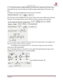
my.ece.utah.eduHomework #1 Fall 2010 3 4. For the circuit below: (a) Find the resistances looking into node 1, R1; node 2, R2; node 3, R3; and node 4, R4. (b) Find the currents I1, I 2, I 3, and I4 in terms of the input current I. (c) Find the voltage at nodes 1,2,3, and 4, that is V1, V2, V3, and V4 in terms of IR.

ECE 5520: Digital Communications Lecture Notes Fall 2009
my.ece.utah.eduA digital communication system conveys discrete-time, discrete-valued information across a physical channel. Information sources might include audio, video, text, or data. They might be continuous-time (analog) signals (audio, images) and even 1-D or 2-D. Or, they may already be digital (discrete-time, discrete-valued). Our
Related documents

Paychex TrueShift User Guide
www.trueshifttimeclock.comTable of Contents TOC Paychex TrueShift User Guide Paychex TrueShift User Guide

2.7V 4-Channel/8-Channel 10-Bit A/D Converters with SPI ...
cdn-shop.adafruit.comJan 02, 2008 · FIGURE 1-1: Serial Interface Timing. Power Requirements Operating Voltage VDD 2.7 — 5.5 V Operating Current IDD —425 225 550 µA VDD = VREF = 5V, DOUT unloaded VDD = VREF = 2.7V, DOUT unloaded Standby Current IDDS —0.005 2 µACS = VDD = 5.0V Electrical Specifications: Unless otherwise indicated, VDD = +2.7V to +5.5V, VSS =GND.

Attention: WORLD backwards, serial 7s from 100
www.admsep.orgFlight of ideas: Rapid shift from one topic to another. Perseveration: R epetition of a particular response (e.g., word or phrase), regardless of the absence or cessation of a stimulus. Thought blocking: Abrupt cessation of speech without explanation in the middle of a sentence
SNx4HC595 8-Bit Shift Registers With 3-State Output ...
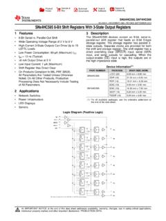
www.ti.comThe SNx4HC595 devices contain an 8-bit, serial-in, parallel-out shift register that feeds an 8-bit D-type storage register. The storage register has parallel 3-state outputs. Separate clocks are provided for both the shift and storage register. The shift register has a direct overriding clear (SRCLR) input, serial (SER)

Introduction • SPI Pin Functionality Features
ww1.microchip.comThe SPI consists of four different signal lines. These lines are the shift clock (SCK), the Master Out Slave In line (MOSI), the Master In Slave Out line (MISO) and the active low Slave Select line ( SS). When the SPI is enabled, the data direction of the MOSI, MISO, SCK, and SS pins are overridden according to the following table. Table 1-1.
8-bit serial-in, serial or parallel-out shift register ...
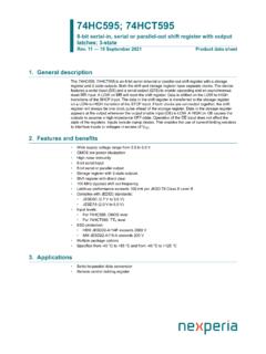
assets.nexperia.comThe 74HC595; 74HCT595 is an 8-bit serial-in/serial or parallel-out shift register with a storage register and 3-state outputs. Both the shift and storage register have separate clocks. The device features a serial input (DS) and a serial output (Q7S) to enable cascading and an asynchronous reset MR input. A LOW on MR will reset the shift register.
Future Technology Devices International Ltd
www.ftdichip.comFTDI FT232B style, asynchronous serial UART interface option with full hardware handshaking and modem interface signals. Fully assisted hardware or X -On / X -Off software handshaking. UART Interface supports 7/8 bit data, 1/2 stop bits, and Odd/Even/Mark/Space/No Parity. Auto -transmit enable control for RS485 serial
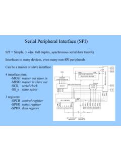
Serial Peripheral Interface (SPI) - College of Engineering
web.engr.oregonstate.eduSerial Peripheral Interface (SPI) Full duplex, synchronous serial data transfer Data is shifted out of the master's (mega128) MOSI pin and in it's MISO pin Data transfer is initiated by simply writing data to the SPI data register. All data movement is coordinated by SCK. Slave select may or may not be used depending on interfacing device.