
D Flip-Flop Design - seloco.com
D Flip-Flop Design Practice - MyCAD 4 Inverter schematic and symbol 1 0 0 1 IN OUT Input Output Logic Symbol Schematic Truth Table L = 0.2um W = 1.6um L = 0.2um
Download D Flip-Flop Design - seloco.com

Information
Domain:
Source:
Link to this page:
Related documents

Xilinx DS060 Spartan and Spartan-XL FPGA Families Data …
www.xilinx.comSpartan and Spartan-XL FPGA Families Data Sheet DS060 (v2.0) March 1, 2013 www.xilinx.com 3 Product Specification R Product Obsolete/Under Obsolescence Spartan and Spartan-XL devices provide system clock

Clock Domain Crossing (CDC) Design & Verification ...
www.sunburst-design.comSNUG Boston 2008 Clock Domain Crossing (CDC) Design & Verification Rev 1.0 Techniques Using SystemVerilog 6 1.0 Introduction In 2001, I presented my first paper on multi-asynchronous clock design.

Get Smart About Reset: Think Local, Not Global - Xilinx
www.xilinx.com6 www.xilinx.com WP272 (v1.0.1) March 7, 2008 R Reset Costs More Than You Think! asynchronous reset signal, the shift register chain begins to fill with 0s each clock cycle. The number of flip-flops in the chain determines the minimum duration of the reset

Synthesis and Scripting Techniques ... - sunburst-design.com
www.sunburst-design.comExpert Verilog, SystemVerilog & Synthesis Training Synthesis and Scripting Techniques for Designing Multi-Asynchronous Clock Designs Clifford E. Cummings, Sunburst Design, Inc. cliffc@sunburst-design…

Lecture 6 Flip-Flop and Clock Design
courses.ece.ubc.caLecture 6 2 RAS Lecture 6 3 Clocked D Flip-flop • Very useful FF • Widely used in IC design for temporary storage of data • May be level-sensitive or edge-triggered
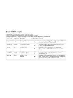
Practical VHDL samples - University of Glasgow
userweb.eng.gla.ac.ukPractical VHDL samples The following is a list of files used as examples in the ESD3 lectures. The files are included overleaf with simulations and also post-synthesis schematics.

Metastability - Engineering Class Home Pages
www-classes.usc.eduINTRODUCTION As system designers continue to push the upper bound of performance, understanding the metastability operation of flip-flops is important to reliability.

Test Generation and Design for Test - Auburn University
www.eng.auburn.eduTest Generation and Design for Test Using Mentor Graphics CAD Tools

SN54AC374, SN74AC374 OCTAL D-TYPE EDGE-TRIGGERED …
www.ti.comsn54ac374, sn74ac374 octal d-type edge-triggered flip-flops with 3-state outputs scas543e − october 1995 - revised october 2003 2 post office box 655303 • dallas, texas 75265