Search results with tag "Flops"

Chapter 18 Sequential Circuits: Flip-flops and Counters
wps.pearsoned.comDesign a counter with the following repeated binary sequence: 0, 4, 2, 1, 6. Use T flip-flops. Solution: Step 1: Since it is a 3-bit counter, the number of flip-flops required is three. Step 2: Let the type of flip-flops be RS flip-flops. Step 3: Let the three flip-flops be A, B and C. Step 4: The state table is as shown in Table 3.1.

FLIP FLOPS - escolaindustrial.com.br
escolaindustrial.com.br2 M-1113A - Flip-Flops 1. Objetivos Verificar experimentalmente o funcionamento dos Flip-Flops. 2. Introdução Teórica Junto com o conceito do que são Flip-Flops, temos que …

Circuits with Flip-Flop = Sequential Circuit Circuit ...
www.cse.psu.edu1 flip-flop => 2 states 2 flip-flops => 4 states 3 flip3 flip-flops => 8 statesflops => 8 states 4 flip-flops => 16 states. Sequential circuit components: Circuit, State Diagram, State Table Sequential circuit components Flip-flop(s) Clock Logic gates Input Output. State diagram:

Flip-Flops and Sequential Circuit Design - UC Santa Barbara
web.ece.ucsb.eduCounter Design with T Flip-Flops Implement design using T Flip-Flops with asynchronous preset and clear Asynchronous preset (PRN) and clear (CLRN) override clock and other inputs Preset : Q →1, Clear : Q →0 Used to initialize system (all flip-flops) to known state Bubbles indicate “low true” or “active low”
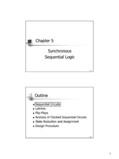
Chapter 5 Synchronous Sequential Logic
www.cse.iitb.ac.inLatches! Flip-Flops! Analysis of Clocked Sequential Circuits! State Reduction and Assignment! Design Procedure. 4 5-7 Latches! The most basic types of flip-flops operate with signal levels! The basic circuits from which all flip-flops are constructed! Useful for …

Modeling Latches and Flip-flops - Xilinx
www.xilinx.com• Model various types of latches • Model flip-flops with control signals Latches Part 1 Storage elements can be classified into latches and flip-flops. Latch is a device with exactly two stable states: high-output and low-output. A latch has a feedback …

Modeling Latches and Flip-flops - Xilinx
www.xilinx.com• Model various types of latches • Model flip-flops with control signals Latches Part 1 Storage elements can be classified into latches and flip-flops. A latch is a device with exactly two stable states: a high-output and a low-output. A latch has a feedback path, so information can be retained by the device.

Latches, the D Flip-Flop & Counter Design
web.ece.ucsb.eduFebruary 6, 2012 ECE 152A - Digital Design Principles 3 Reading Assignment Brown and Vranesic (cont) 7Flip-Flops, Registers, Counters and a Simple Processor (cont) 7.4 Master-Slave and Edge-Triggered D Flip-Flops 7.4.1 Master-Slave D Flip-Flop 7.4.2 Edge-Triggered D Flip-Flop 7.4.3 D Flip-Flop with Clear and Preset 7.4.4 Flip-Flop Timing Parameters (2nd edition)

Metastability and Synchronizers A Tutorial
webee.technion.ac.ilIn flip-flops, metastability means indecision of whether the output should be ‗0‘ or ‗1‘. Here is a simplified circuit analysis model. The typical flip-flops in Figure 2 comprise master and slave latches and decoupling inverters. In metastability, the voltage levels of nodes A,B of the master latch are roughly mid-way between logic ‗1 ...

Latches and Flip-Flops
www.csie.ntu.edu.twTiming Diagram for D Flip-Flop with Asynchronous Clear and Preset ꣣ꚳꭄꙐꡂ뉍낣ꥍ륷롭뿩ꑊ냊ꝀꪺDꮬꖿ뺹 껉Ꟈ맏ꅃ Unit 11 Latches and Flip-Flops 28 Review Question ꅩ닟썄豶螰ꅪ(page 312)ꅇ a) Complete the following timing diagram for a J-K flip-flop with a falling-edge trigger and asynchronous ClrN and PreN inputs.

RI5CY: User Manual - PULP platform
www.pulp-platform.orgflip-flops, except for the register file, which can be implemented either with latches or with flip-flops. See Chapter 8 for more details about the register file. The core occupies an area of about 50 kGE when the latch based register file is used. With the FPU, the core area increases to about 90 kGE (30kGE FPU, 10kGE additional register file).

ELEVATOR CONTROL CIRCUIT
eie.uonbi.ac.kecircuits. In a synchronous sequential circuit, changes of state are only allowed to happen at times synchronous to a special timing signal, called the clock. The simplest synchronous circuit is a one-bit storage element, which is also referred to as a flip-flop. There are four popular types of flip-flops i.e. JK, D, T and SR flip-flops ...

Chapter 6 Synchronous Sequential Circuits
my.ece.utah.eduSequential circuits can be: ! • Synchronous – where flip-flops are used to ... Choose the type of flip-flops to be used. 7. Derive the logic expressions needed to implement the circuit. ... Derivation of next-state expressions for the sequential circuit in Figure 6.18. w 00 01 11 10 0 1 1 y 2 y 1 Y 1 = wy 2 + y 1 y w 00 01 11 10 0 1 1 y 2 y 1 Y

Sequential Circuit Design - University of Pittsburgh
sites.pitt.eduElec 326 14 Sequential Circuit Design Select the Flip-Flop Type The four main types of flip-flops are SR, D, T and JK. The choice of flip-flop type can affect the complexity of the combinational logic in the resulting sequential circuit. Of three common types, the most versatile is the JK, since it can be easily converted into the other two.

Survey Research - SAGE Publications Inc
www.sagepub.comlikely to be a flop. Such flops are too common for comfort, and the responsible survey researcher must take ... A survey should be guided by a clear conception of the research problem under investigation and the popula - tion to be sampled. Throughout the process of questionnaire design, the research objective should be the pri - ...

CHAPTER VIII FINITE STATE MACHINES (FSM) - gatech.edu
limsk.ece.gatech.edu• Flip-flops, registers, and latches that are enabled/controlled with a signal derived from clock form a synchronous sequential system. • Asynchronous sequential system • Behaviour depends on inputs at any instant of time. • Latches without control signals behave in …

Verilog HDL Coding - Cornell University
people.ece.cornell.eduR 7.10.12 Use nonblocking assignments when inferring flip-flops and latches R 7.10.13 Drive all unused module inputs G 7.10.14 Connect unused module outputs R 7.10.15 Do not infer latches in functions R 7.10.16 Use of casex is not allowed R …

Lecture 6 Flip-Flop and Clock Design
courses.ece.ubc.caRequirements in Flip-Flop Design • Minimize FF overhead: small clk-q delay, tsetup, thold times • Minimize power – expensive packages and cooling systems – flops up to 20% of total power of high-performance systems • High driving capability – Typical flip-flop load in a 0.18 µm CMOS ranges from 50fF to
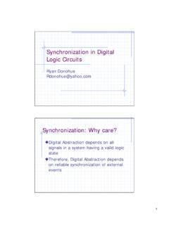
Synchronization in Digital Logic Circuits
web.stanford.edu6 SYNC Flip Flop SYNC Flip Flops are available in some ASIC libraries n Better MTBF characteristics due to high gain in the feedback path n Very large (5x regular FF) and very high power D Q D Q SIG META CLK SIG1 SYNC Vin Vout VTC of regular FF series inverters
Massachusetts Institute of Technology
web.mit.edu6.111 Spring 2007 Problem Set 1 3 Problem 5: Setup and Hold Times for D Flip-Flop (Flip-flops will be covered in lecture 4) 1) Let a D latch be implemented using a mux and realized as follows: You may assume the following: a) G and G are complements and have zero skew, i.e. …

DESIGNING SEQUENTIAL LOGIC CIRCUITS
bwrcs.eecs.berkeley.eduImplementation techniques for flip-flops, latches, oscillators, pulse generators, n and Schmitt triggers n Static versus dynamic realization Choosing clocking strategies 7.1 Introduction 7.2 Timing Metrics for Sequential Circuits 7.3 Classification of Memory Elements 7.4 Static Latches and Registers

Presettable synchronous 4-bit binary counter ... - Nexperia
assets.nexperia.comcarry. Synchronous operation is provided by having all flip-flops clocked simultaneously on the positive-going edge of the clock (CP). The outputs (Q0 to Q3) of the counters may be preset to a HIGH or LOW. A LOW at the parallel enable input (PE) disables the counting action. It causes

Octal D-Type Transparent Latches And Edge-Triggered Flip ...
www.ti.comThe eight latches of the ’LS373 and ’S373 are transparent D-type latches, meaning that while the enable (C or CLK) input is high, the Q outputs follow the data (D) inputs. When C or CLK is taken low, the output is latched at the level of the data that was set up. The eight flip-flops of the ’LS374 and ’S374 are edge-triggered D-type ...

MC74HC74A - Dual D Flip-Flop with Set and Reset
www.onsemi.comDual D Flip-Flop with Set and Reset High−Performance Silicon−Gate CMOS The MC74HC74A is identical in pinout to the LS74. The device inputs are compatible with standard CMOS outputs; with pullup resistors, they are compatible with LSTTL outputs. This device consists of two D flip−flops with individual Set, Reset, and Clock inputs.

VHDL: Modeling RAM and Register - Auburn University
www.eng.auburn.eduRandom logic using flip-flops or latches Register files in datapaths RAM standard components RAM compilers Computer “register files” are often just multi-port RAMs ARM CPU: 32-bit registers R0-R15 => 16 x 32 RAM MIPS CPU: 32-bit registers R0-R31 => 32 x 32 RAM Communications systems often use dual-port RAMs as
CONTADORES - unican.es
personales.unican.esentrada J y otro para la entrada K de cada flip-flop. Habrá que realizar tantos mapas de Karnaugh como entradas de flip-flops. Estado actual Estado siguiente Entradas del flip-flop Q2 Q1 Q0 Q2 Q1 Q0 J2 K2 J1 K1 J0 K0 0 0 0 0 0 1 0 X 0 X 1 X 0 0 1 0 1 0 0 X 1 X X 1 0 1 0 0 1 1 0 X X 0 1 X 0 1 1 1 0 0 1 X X 1 X 1 1 0 0 1 0 1 X 0 0 X 1 X

Defense-Grade 7 Series FPGAs Overview (DS185)
www.xilinx.comFour of the eight flip-flops per slice (one per LUT) can optionally be configured as latches. Between 25–50% of all slices can also use their LUTs as distri buted 64-bit RAM or as 32-bit shift registers (SRL32) or as two SRL16s. Modern synthesis tools take advantage of these hi ghly efficient logic, arithmetic, and memory features.

Modeling Latches and Flip-flops - Xilinx
www.xilinx.comflip-flop can be viewed as a memory cell or a delay line. The active edge in a flip-flop could be rising or falling. The following figure shows rising (also called positive) edge triggered D flip-flop and falling (negative edge) triggered D flip-flop. The positive edge triggered D flip-flop can be modeled using behavioral modeling as shown below.

Circuitos Seqüenciais Latches e Flip-Flops
www.univasf.edu.breno m inação l a tch é susada pa ra c cu os plif cados. T ermo Flip f lop usado pa ra atches com óg io e c cu o m s complexo. • Tem a função de armazenar níveis lógicos temporariamente, funcionando como uma memória. • É implementado a partir de portas lógicas, através de conexões de realimentação.

ICL8038 - MIT
www.mit.eduthat the flip-flop is in a state such that current source #2 is off, and the capacitor is charged with a current I, the voltage across the capacitor rises linearly with time. When this voltage reaches the level of comparator #1 (set at 2/3 of the supply voltage), the flip-flop is triggered, changes states, and releases current source #2.

RISC-V CPU Datapath, Control Intro
inst.eecs.berkeley.edu•Similar to D flip-flop except: –N-bit input and output buses –Write Enable input •Write Enable: –De-asserted (0): Data Out will not change –Asserted (1): Data In value placed onto Data Out after CLK trigger 36 CLK Data In Write Enable N N Data Out 7/09/2018 CS61C Su18 - Lecture 11
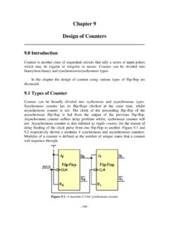
Chapter 9 Design of Counters - Universiti Tunku Abdul Rahman
staff.utar.edu.mylearnt earlier in Chapter 7, the excitation or characteristic table of SR flip-flop, D flip-flip, JK flip-flop, and T flip-flop are shown in Fig. 9.7. and 9.8 respectively. Q t is denotes the output of the present state and Q t+1 denotes the output of next state.

Dual D-type flip-flop
assets.nexperia.comDual D-type flip-flop Rev. 10 — 23 November 2021 Product data sheet 1. General description The HEF4013B is a dual D-type flip-flop with set and reset; positive-edge trigger. Inputs include clamp diodes. This enables the use of current limiting resistors to interface inputs to voltages in excess of VDD. 2. Features and benefits
An Introduction to Business Research
study.sagepub.comeffectively, researchers must have a clear set of research questions. The importance ... Design guru Stephen Bayley condemned it as ‘a puerile mess, an artistic flop and a commercial scandal’. An online petition to get the logo scrapped received thousands of signatures, while

FPGA Logic Cells Comparison - Sharif
ee.sharif.edu• D flip-flop or latch. Fig. 3: A simplified diagram of the Altera ALM 4-input LUT 3-input LUT 3-input LUT 4-input LUT 3-input LUT 3-input LUT Interconnect ... 1-CORE Technologies is a leading Russian electronics design company providing high-quality and cost-effective FPGA and ASIC design services. Address: 24 Radio str., Moscow, Russia, 105005

SN54/74LS192 SN54/74LS193 PRESETTABLE BCD/DECADE …
ece-classes.usc.edutwos or not at all, depending on the state of the first flip-flop, which cannot toggle as long as either Clock input is LOW. The Terminal Count Up (TCU) and Terminal Count Down (TCD) outputs are normally HIGH. When a circuit has reached the maximum count state (9 for the LS192, 15 for the LS193), the next HIGH-to-LOW transition of the Count Up ...

D Flip-Flop Design - seloco.com
www.seloco.comD Flip-Flop Design Practice - MyCAD 4 Inverter schematic and symbol 1 0 0 1 IN OUT Input Output Logic Symbol Schematic Truth Table L = 0.2um W = 1.6um L = 0.2um

Metastability - University of Southern California
www-classes.usc.edutypically described by four measurements of flip-flop performance — MTBF, T, To and tr. MTBF is the “mean-time-between-failure” of a flip-flop. where tr is metastability resolution time, maximum time the output can remain metastable without causing synchronizer failure. …

Hobby Servo Fundamentals - Princeton University
www.princeton.eduflip-flop that toggles the direction the current flows through the motor. The outputs of the flip-flop drive an H-Bridge circuit that handles the high current going through the motor. If you were going to try to build a circuit to take a PWM signal and convert it to a motor position, you'd probably end up with a fairly large circuit.

NL17SZ74 - Single D Flip Flop - ON Semiconductor
www.onsemi.comNL17SZ74 www.onsemi.com 2 MAXIMUM RATINGS Symbol Parameter Value Units VCC DC Supply Voltage −0.5 to +7.0 V VI DC Input Voltage −0.5 to +7.0 V VO DC Output Voltage − Output in High or Low State (Note 1) −0.5 to VCC +0.5 V IIK DC Input Diode Current VI < GND −50 mA IOK DC Output Diode Current VO < GND −50 mA IO DC Output Sink Current ±50 mA ICC DC Supply Current Per …
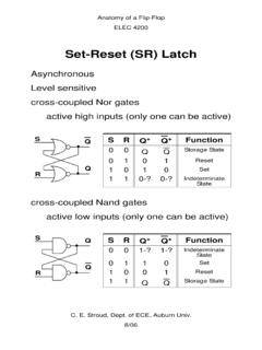
Set-Reset (SR) Latch - Auburn University
www.eng.auburn.eduC. E. Stroud, Dept. of ECE, Auburn Univ. 8/06 Anatomy of a Flip-Flop ELEC 4200 Timing Considerations Set-up time (tsu)= minimum time input data must be valid before active edge of clock
Hypocritical Flip-Flop, or Courageous Evolution?
www.apa.orgDespite the appeal of the hypocrisy hypothesis, therefore, it also seems conceivable that, at least under certain conditions, audience members give extra credit to initially moral mind changers.

Flip-flop e loro applicazioni - Roberto Roncella …
roncella.iet.unipi.itFlip-flop e loro applicazioni Reti sequenziali elementari (6) L'elemento bistabile Latch o flip-flop trasparenti Temporizzazione dei flip-flop trasparenti

SystemVerilog Assertions Design Tricks and SVA Bind Files
www.sunburst-design.comMar 24, 2009 · exceptionally incompetent engineer has coded a very flawed D-flip-flop as shown in Example 1: module dff (output logic q, input d, clk, rst_n); assign q = d; // This is clearly a mistake!! endmodule Example 1 - Incorrectly coded D-flip-flop model To this dff module, let's first add a concurrent assertion with no label, but we will include an
Similar queries
Chapter 18 Sequential Circuits: Flip-flops and, Design, Flip, Flops, Flip-Flop, Preset and clear, Preset, And clear, Clear, Latches, 7 Latches, Modeling Latches and Flip-flops, Xilinx, Latches and flip, Flop, RI5CY: User Manual, Circuits, Sequential, Chapter, Sequential circuits, SAGE Publications Inc, Verilog, Clock, Synchronization in Digital Logic Circuits, Massachusetts Institute of Technology, DESIGNING SEQUENTIAL LOGIC CIRCUITS, Type Transparent Latches And Edge-Triggered Flip, Modeling, CONTADORES, Circuitos Seqüenciais Latches e Flip-Flops, Plif, D flip, FPGA Logic Cells Comparison, D Flip-Flop Design, Metastability, Princeton University, NL17SZ74 - Single D Flip Flop, Hypocritical Flip-Flop, or Courageous Evolution