Search results with tag "Flip flops"

Circuits with Flip-Flop = Sequential Circuit Circuit ...
www.cse.psu.edu1 flip-flop => 2 states 2 flip-flops => 4 states 3 flip3 flip-flops => 8 statesflops => 8 states 4 flip-flops => 16 states. Sequential circuit components: Circuit, State Diagram, State Table Sequential circuit components Flip-flop(s) Clock Logic gates Input Output. State diagram:

Latches, the D Flip-Flop & Counter Design
web.ece.ucsb.eduFebruary 6, 2012 ECE 152A - Digital Design Principles 3 Reading Assignment Brown and Vranesic (cont) 7Flip-Flops, Registers, Counters and a Simple Processor (cont) 7.4 Master-Slave and Edge-Triggered D Flip-Flops 7.4.1 Master-Slave D Flip-Flop 7.4.2 Edge-Triggered D Flip-Flop 7.4.3 D Flip-Flop with Clear and Preset 7.4.4 Flip-Flop Timing Parameters (2nd edition)

Modeling Latches and Flip-flops - Xilinx
www.xilinx.comflip-flop can be viewed as a memory cell or a delay line. The active edge in a flip-flop could be rising or falling. The following figure shows rising (also called positive) edge triggered D flip-flop and falling (negative edge) triggered D flip-flop. The positive edge triggered D flip-flop can be modeled using behavioral modeling as shown below.

Modeling Latches and Flip-flops - Xilinx
www.xilinx.comflip-flop can be viewed as a memory cell or a delay line. The active edge in a flip-flop could be rising or falling. The following figure shows rising (also called positive) edge triggered D flip-flop and falling (negative edge) triggered D flip-flop. The positive edge triggered D flip-flop can be modeled using behavioral modeling as shown ...

MC74HC74A - Dual D Flip-Flop with Set and Reset
www.onsemi.comDual D Flip-Flop with Set and Reset High−Performance Silicon−Gate CMOS The MC74HC74A is identical in pinout to the LS74. The device inputs are compatible with standard CMOS outputs; with pullup resistors, they are compatible with LSTTL outputs. This device consists of two D flip−flops with individual Set, Reset, and Clock inputs.

Lecture 6 Flip-Flop and Clock Design
courses.ece.ubc.caRequirements in Flip-Flop Design • Minimize FF overhead: small clk-q delay, tsetup, thold times • Minimize power – expensive packages and cooling systems – flops up to 20% of total power of high-performance systems • High driving capability – Typical flip-flop load in a 0.18 µm CMOS ranges from 50fF to

Get Smart About Reset: Think Local, Not Global - …
www.xilinx.com6 www.xilinx.com WP272 (v1.0.1) March 7, 2008 R Reset Costs More Than You Think! asynchronous reset signal, the shift register chain begins to fill with 0s each clock cycle. The number of flip-flops in the chain determines the minimum duration of the reset

Flip-Flops and Sequential Circuit Design
web.ece.ucsb.eduFebruary 13, 2012 ECE 152A - Digital Design Principles 2 Reading Assignment Brown and Vranesic 7Flip-Flops, Registers, Counters and a Simple Processor 7.5 T Flip-Flop 7.5.1 Configurable Flip-Flops 7.6 JK Flip-Flop 7.7 Summary of Terminology 7.8 Registers 7.8.1 Shift Register 7.8.2 Parallel-Access Shift Register

Dual D-type flip-flop
assets.nexperia.comDual D-type flip-flop Rev. 10 — 23 November 2021 Product data sheet 1. General description The HEF4013B is a dual D-type flip-flop with set and reset; positive-edge trigger. Inputs include clamp diodes. This enables the use of current limiting resistors to interface inputs to voltages in excess of VDD. 2. Features and benefits

Metastability - University of Southern California
www-classes.usc.edutypically described by four measurements of flip-flop performance — MTBF, T, To and tr. MTBF is the “mean-time-between-failure” of a flip-flop. where tr is metastability resolution time, maximum time the output can remain metastable without causing synchronizer failure. …
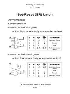
Set-Reset (SR) Latch - Auburn University
www.eng.auburn.eduC. E. Stroud, Dept. of ECE, Auburn Univ. 8/06 Anatomy of a Flip-Flop ELEC 4200 Timing Considerations Set-up time (tsu)= minimum time input data must be valid before active edge of clock