Transcription of ICL8038 - MIT
1 ICL8038 . Semiconductor September 1998 File Number Precision Waveform Generator/Voltage Features Controlled Oscillator Low Frequency Drift with Temperature ..250ppm/oC. The ICL8038 waveform generator is a monolithic integrated Low Distortion.. 1% (Sine Wave Output). circuit capable of producing high accuracy sine, square, High Linearity .. (Triangle Wave Output). triangular, sawtooth and pulse waveforms with a minimum of external components. The frequency (or repetition rate) can Wide Frequency Range .. to 300kHz be selected externally from to more than 300kHz Variable Duty Cycle .. 2% to 98%.
2 Using either resistors or capacitors, and frequency modulation and sweeping can be accomplished with an High Level Outputs .. TTL to 28V. external voltage. The ICL8038 is fabricated with advanced Simultaneous Sine, Square, and Triangle Wave monolithic technology, using Schottky barrier diodes and thin Outputs film resistors, and the output is stable over a wide range of Easy to Use - Just a Handful of External Components temperature and supply variations. These devices may be Required interfaced with phase locked loop circuitry to reduce temperature drift to less than 250ppm/oC. Ordering Information PART NUMBER STABILITY TEMP.
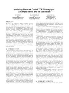
3 RANGE (oC) PACKAGE PKG. NO. ICL8038 CCPD 250ppm/oC (Typ) 0 to 70 14 Ld PDIP ICL8038 CCJD 250ppm/oC (Typ) 0 to 70 14 Ld CERDIP ICL8038 BCJD 180ppm/oC (Typ) 0 to 70 14 Ld CERDIP ICL8038 ACJD 120ppm/oC (Typ) 0 to 70 14 Ld CERDIP Pinout Functional Diagram ICL8038 . V+. (PDIP, CERDIP) 6. TOP VIEW CURRENT. SOURCE. #1 COMPARATOR. I #1. SINE WAVE 1 14 NC 10. ADJUST. SINE 2I. 2 13 NC C COMPARATOR. WAVE OUT. #2. TRIANGLE. 3 12 SINE WAVE. OUT ADJUST. DUTY CYCLE 4 11 V- OR GND. FREQUENCY. ADJUST 5 10 TIMING CURRENT. CAPACITOR SOURCE flip -FLOP. 6 9 SQUARE #2. V+. WAVE OUT V- OR GND. FM SWEEP 11. FM BIAS 7 8.
4 INPUT. SINE. BUFFER BUFFER CONVERTER. 9 3 2. 1 CAUTION: These devices are sensitive to electrostatic discharge; follow proper IC Handling Procedures. Copyright Harris Corporation 1998. ICL8038 . Absolute Maximum Ratings Thermal Information Supply Voltage (V- to V+).. 36V Thermal Resistance (Typical, Note 1) JA (oC/W) JC (oC/W). Input Voltage (Any Pin) .. V- to V+ CERDIP Package.. 75 20. Input Current (Pins 4 and 5).. 25mA PDIP Package .. 115 N/A. Output Sink Current (Pins 3 and 9) .. 25mA Maximum Junction Temperature (Ceramic Package) ..175oC. Maximum Junction Temperature (Plastic Package).
5 150oC. Operating Conditions Maximum Storage Temperature Range .. -65oC to 150oC. Maximum Lead Temperature (Soldering 10s) .. 300oC. Temperature Range ICL8038AC, ICL8038BC, ICL8038CC .. 0oC to 70oC. Die Characteristics Back Side Potential .. V- CAUTION: Stresses above those listed in Absolute Maximum Ratings may cause permanent damage to the device. This is a stress only rating and operation of the device at these or any other conditions above those indicated in the operational sections of this specification is not implied. NOTE: 1. JA is measured with the component mounted on an evaluation PC board in free air.
6 Electrical Specifications VSUPPLY = 10V or +20V, TA = 25oC, RL = 10k , Test Circuit Unless Otherwise Specified ICL8038CC ICL8038BC ICL8038AC. TEST. PARAMETER SYMBOL CONDITIONS MIN TYP MAX MIN TYP MAX MIN TYP MAX UNITS. Supply Voltage Operating Range VSUPPLY. V+ Single Supply +10 - +30 +10 - +30 +10 - +30 V. V+, V- Dual Supplies 5 - 15 5 - 15 5 - 15 V. Supply Current ISUPPLY VSUPPLY = 10V 12 20 - 12 20 - 12 20 mA. (Note 2). FREQUENCY CHARACTERISTICS (All Waveforms). Max. Frequency of Oscillation fMAX 100 - - 100 - - 100 - - kHz Sweep Frequency of FM Input fSWEEP - 10 - - 10 - - 10 - kHz Sweep FM Range (Note 3) - 35:1 - - 35:1 - - 35:1 - FM Linearity 10:1 Ratio - - - - - - %.
7 Frequency Drift with f/ T 0oC to 70oC - 250 - - 180 - - 120 ppm/oC. Temperature (Note 5). Frequency Drift with Supply Voltage f/ V Over Supply - - - - - %/V. Voltage Range OUTPUT CHARACTERISTICS. Square Wave Leakage Current IOLK V9 = 30V - - 1 - - 1 - - 1 A. Saturation Voltage VSAT ISINK = 2mA - - - V. Rise Time tR RL = - 180 - - 180 - - 180 - ns Fall Time tF RL = - 40 - - 40 - - 40 - ns Typical Duty Cycle Adjust D 2 98 2 - 98 2 - 98 %. (Note 6). Triangle/Sawtooth/Ramp - Amplitude VTRIAN- RTRI = 100k - - - xVSUPPLY. GLE. Linearity - - - - - - %. Output Impedance ZOUT IOUT = 5mA - 200 - - 200 - - 200.
8 2. ICL8038 . Electrical Specifications VSUPPLY = 10V or +20V, TA = 25oC, RL = 10k , Test Circuit Unless Otherwise Specified (Continued). ICL8038CC ICL8038BC ICL8038AC. TEST. PARAMETER SYMBOL CONDITIONS MIN TYP MAX MIN TYP MAX MIN TYP MAX UNITS. Sine Wave Amplitude VSINE RSINE = 100k - - - xVSUPPLY. THD THD RS = 1M - 5 - 3 - %. (Note 4). THD Adjusted THD Use Figure 4 - - - - - - %. NOTES: 2. RA and RB currents not included. 3. VSUPPLY = 20V; RA and RB = 10k , f 10kHz nominal; can be extended 1000 to 1. See Figures 5A and 5B. 4. 82k connected between pins 11 and 12, Triangle Duty Cycle set at 50%.
9 (Use RA and RB.). 5. Figure 1, pins 7 and 8 connected, VSUPPLY = 10V. See Typical Curves for vs VSUPPLY. 6. Not tested, typical value for design purposes only. Test Conditions PARAMETER RA RB RL C SW1 MEASURE. Supply Current 10k 10k 10k Closed Current Into Pin 6. Sweep FM Range (Note 7) 10k 10k 10k Open Frequency at Pin 9. Frequency Drift with Temperature 10k 10k 10k Closed Frequency at Pin 3. Frequency Drift with Supply Voltage (Note 8) 10k 10k 10k Closed Frequency at Pin 9. Output Amplitude (Note 10). Sine 10k 10k 10k Closed Pk-Pk Output at Pin 2. Triangle 10k 10k 10k Closed Pk-Pk Output at Pin 3.
10 Leakage Current (Off) (Note 9) 10k 10k Closed Current into Pin 9. Saturation Voltage (On) (Note 9) 10k 10k Closed Output (Low) at Pin 9. Rise and Fall Times (Note 11) 10k 10k Closed Waveform at Pin 9. Duty Cycle Adjust (Note 11). Max 50k ~ 10k Closed Waveform at Pin 9. Min ~25k 50k 10k Closed Waveform at Pin 9. Triangle Waveform Linearity 10k 10k 10k Closed Waveform at Pin 3. Total Harmonic Distortion 10k 10k 10k Closed Waveform at Pin 2. NOTES: 7. The hi and lo frequencies can be obtained by connecting pin 8 to pin 7 (fHI) and then connecting pin 8 to pin 6 (fLO). Otherwise apply Sweep Voltage at pin 8 (2/3 VSUPPLY +2V) VSWEEP VSUPPLY where VSUPPLY is the total supply voltage.