
ICL8038 - MIT
that the flip-flop is in a state such that current source #2 is off, and the capacitor is charged with a current I, the voltage across the capacitor rises linearly with time. When this voltage reaches the level of comparator #1 (set at 2/3 of the supply voltage), the flip-flop is triggered, changes states, and releases current source #2.
Download ICL8038 - MIT

Information
Domain:
Source:
Link to this page:
Documents from same domain
Modeling Network Coded TCP Throughput: A …
www.mit.eduModeling Network Coded TCP Throughput: A Simple Model and its Validation MinJi Kim MIT Cambridge, MA 02139 minjikim@mit.edu Muriel Médard MIT Cambridge, MA 02139
LM108/LM208/LM308 Operational Amplifiers - …
www.mit.eduAbsolute Maximum Ratings If Military/Aerospace specified devices are required, please contact the National Semiconductor Sales Office/ Distributors for …
Chapter 8 New Product Development* - mit.edu
www.mit.eduUnfortunately, new product development is an extremely challenging and complex process. Innovation is inherently risky, and firms may invest considerable time and money in
The Voice of the Customer
www.mit.eduQuality Function Deployment (QFD) (see WIEM05-023), or the setting of detailed design specifications (see WIEM05-049). The Voice of the Customer process has important outputs and benefits for product developers.

Note on Conjoint Analysis - mit.edu
www.mit.eduM I T S L O A N C O U R S E W A R E > P. 1 Note on Conjoint Analysis John R. Hauser Suppose that you are working for one of the primary brands of global
a Ultralow Offset Voltage Operational Amplifiers OP07
www.mit.eduREV.A Information furnished by Analog Devices is believed to be accurate and reliable. However, no responsibility is assumed by Analog Devices for its
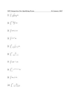
MIT Integration Bee Qualifying Exam 24 January 2017
www.mit.eduMIT Integration Bee Qualifying Exam 24 January 2017 1 Z x2 p x3 +2 dx 2 Z 1 1 logx x2 dx 3 Z sech(x)dx 4 Z x3ex2 dx 5 Z 2 1 1 x p x2 1 dx 6 Z 1 1 dx x(x2 +1) 7 Z cosh 1 xdx 8 Z 1 1 e 2x2 5x 3 dx 9 Z sin p xdx 10 Z 1 0 dx (x+1=x)2

Efficient wireless non-radiative mid-range energy …
www.mit.eduEfficient wireless non-radiative mid-range energy transfer Aristeidis Karalis a,*, J.D. Joannopoulos b, Marin Soljacˇic´ b a Department of Electrical Engineering and Computer Science, Massachusetts Institute of Technology,

Freedom of Association Is Not the Answer* - mit.edu
www.mit.eduFine Freedom of Association Is Not the Answer 339 dom of association and exclusion: few would argue with Amy Gutmann’s statement that “the freedom to associate . . . entails the freedom to
a Operational Amplifier Low-Noise, Precision OP27
www.mit.eduREV. C –3– OP27 ELECTRICAL CHARACTERISTICS (@ V S = ±15 V, –55 C £ T A £ 125 C, unless otherwise noted.) OP27A OP27C Parameter Symbol Conditions Min Typ Max Min Typ Max Unit INPUT OFFSET
Related documents

SystemVerilog Assertions Design Tricks and SVA Bind Files
www.sunburst-design.comMar 24, 2009 · exceptionally incompetent engineer has coded a very flawed D-flip-flop as shown in Example 1: module dff (output logic q, input d, clk, rst_n); assign q = d; // This is clearly a mistake!! endmodule Example 1 - Incorrectly coded D-flip-flop model To this dff module, let's first add a concurrent assertion with no label, but we will include an

FPGA Logic Cells Comparison - Sharif
ee.sharif.edu• D flip-flop or latch. Fig. 3: A simplified diagram of the Altera ALM 4-input LUT 3-input LUT 3-input LUT 4-input LUT 3-input LUT 3-input LUT Interconnect ... 1-CORE Technologies is a leading Russian electronics design company providing high-quality and cost-effective FPGA and ASIC design services. Address: 24 Radio str., Moscow, Russia, 105005

Sequential Circuit Design - University of Pittsburgh
sites.pitt.eduElec 326 14 Sequential Circuit Design Select the Flip-Flop Type The four main types of flip-flops are SR, D, T and JK. The choice of flip-flop type can affect the complexity of the combinational logic in the resulting sequential circuit. Of three common types, the most versatile is the JK, since it can be easily converted into the other two.
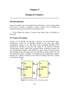
Chapter 9 Design of Counters - Universiti Tunku Abdul Rahman
staff.utar.edu.mylearnt earlier in Chapter 7, the excitation or characteristic table of SR flip-flop, D flip-flip, JK flip-flop, and T flip-flop are shown in Fig. 9.7. and 9.8 respectively. Q t is denotes the output of the present state and Q t+1 denotes the output of next state.

Hobby Servo Fundamentals - Princeton University
www.princeton.eduflip-flop that toggles the direction the current flows through the motor. The outputs of the flip-flop drive an H-Bridge circuit that handles the high current going through the motor. If you were going to try to build a circuit to take a PWM signal and convert it to a motor position, you'd probably end up with a fairly large circuit.

Modeling Latches and Flip-flops - Xilinx
www.xilinx.comThe D flip-flop can be viewed as a memory cell or a delay line. The active edge in a flip-flop could be rising or falling. The following figure shows rising (also called positive) edge triggered D flip-flop and falling (negative edge) triggered D flip-flop. The positive edge triggered D flip-flop can be modeled using behavioral modeling as ...

RISC-V CPU Datapath, Control Intro
inst.eecs.berkeley.edu•Similar to D flip-flop except: –N-bit input and output buses –Write Enable input •Write Enable: –De-asserted (0): Data Out will not change –Asserted (1): Data In value placed onto Data Out after CLK trigger 36 CLK Data In Write Enable N N Data Out 7/09/2018 CS61C Su18 - Lecture 11

Chapter 18 Sequential Circuits: Flip-flops and Counters
wps.pearsoned.comDesign a counter with the following repeated binary sequence: 0, 4, 2, 1, 6. Use T flip-flops. Solution: Step 1: Since it is a 3-bit counter, the number of flip-flops required is three. Step 2: Let the type of flip-flops be RS flip-flops. Step 3: Let the three flip-flops be A, B and C. Step 4: The state table is as shown in Table 3.1.

Modeling Latches and Flip-flops - Xilinx
www.xilinx.comThe D flip-flop captures the value of the D-input at a definite portion of the clock cycle (such as the rising edge of the clock). That captured value becomes the Q output. At other times, the output Q does not change. The D flip-flop can be viewed as a memory cell or a delay line. The active edge in a flip-flop could be rising or falling.