Transcription of a Operational Amplifier Low-Noise, Precision OP27
1 AOP27 Information furnished by Analog Devices is believed to be accurate andreliable. However, no responsibility is assumed by Analog Devices for itsuse, nor for any infringements of patents or other rights of third parties thatmay result from its use. No license is granted by implication or otherwiseunder any patent or patent rights of Analog Devices. Trademarks andregistered trademarks are the property of their respective Technology Way, Box 9106, Norwood, MA 02062-9106, : 781/329-4700 : 781/326-8703 2003 Analog Devices, Inc.
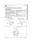
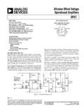
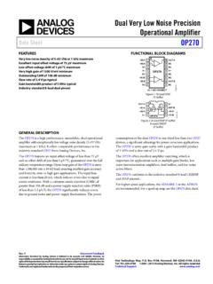
2 All rights CLow-Noise, PrecisionOperational AmplifierPIN CONNECTIONSTO-99(J-Suffix)V+OUTNC4V (CASE)BALBAL 1 IN 2+IN 3OP27NC = NO CONNECTFEATURESLow Noise: 80 nV p-p ( Hz to 10 Hz), 3 nV/ HzLow Drift: V/ CHigh Speed: V/ s Slew Rate, 8 MHz GainBandwidthLow VOS: 10 VExcellent CMRR: 126 dB at VCM of 11 VHigh Open-Loop Gain: MillionFits 725, OP07, 5534A SocketsAvailable in Die FormGENERAL DESCRIPTIONThe OP27 Precision Operational Amplifier combines the lowoffset and drift of the OP07 with both high speed and low down to 25 mV and maximum drift of mV/ C, makesthe OP27 ideal for Precision instrumentation low noise, en = nV/ Hz, at 10 Hz, a low 1/fnoise corner frequency of Hz, and high gain ( million),allow accurate high-gain amplification of low-level signals.
3 Again-bandwidth product of 8 MHz and a V/msec slew rateprovides excellent dynamic accuracy in high-speed, data-acquisition low input bias current of 10 nA is achieved by use of abias-current-cancellation circuit. Over the military temperaturerange, this circuit typically holds IB and IOS to 20 nA and 15 nA, output stage has good load driving capability. A guaranteedswing of 10 V into 600 W and low output distortion make theOP27 an excellent choice for professional audio applications.(Continued on page 7)SIMPLIFIED SCHEMATICV V+Q2BR2*Q3Q2AQ1AQ1BR4R1*R318 VOS AND R2 ARE PERMANENTLYADJUSTED AT WAFER TEST FORMINIMUM OFFSET VOLTAGE.
4 *NONINVERTINGINPUT (+)INVERTINGINPUT ( )Q6Q21C2R23R24Q23Q24Q22R5Q11 Q12Q27Q28C1R9R12C3C4Q26Q20Q19Q46Q45 OUTPUT8-Pin Hermetic DIP(Z-Suffix)Epoxy Mini-DIP(P-Suffix)8-Pin SO(S-Suffix)87651234NC = NO CONNECTVOS TRIM IN+INVOS TRIMV+OUTNCV OP27 REV. C 2 OP27 electrical CHARACTERISTICS OP27A/E OP27F OP27C/GParameterSymbolConditionsMinTypMa xMinTypMaxMinTypMaxUnitINPUT OFFSETVOLTAGE1 VOS1025206030100mVLONG-TERM VOSSTABILITY2, 3 OFFSETCURRENTIOS7359501275 nAINPUT BIASCURRENTIB 10 40 12 55 15 80nAINPUT NOISEVOLTAGE3, 4en Hz to 10 p-pINPUT NOISEenfO = 10 HzVoltage Density3fO = 30 HzfO = 1000 HzINPUT NOISEinfO = 10 HzCurrent Density3.
5 5fO = 30 HzfO = 1000 VOLTAGERANGEIVR RATIO CMRRVCM = 11 V114126106123100120dBPOWER SUPPLYPSRRVS = 4 VREJECTION RATIOto 18 V110110220mV/VLARGE-SIGNALAVORL 2 kW,VOLTAGE GAINVO = 10 V10001800100018007001500V/mVRL 600 W,VO = 10 V800150080015006001500V/mVOUTPUTVOLTAGE SWINGVORL 2 kW 600 W RATE7 SRRL 2 = 0, IO = 07070 70 WPOWERCONSUMPTIONPdVO9014090140100170mWO FFSETADJUSTMENTRANGERP = 10 kW offset voltage measurements are performed ~ seconds after application of power. A/E grades guaranteed fully warmed input offset voltage stability refers to the average trend line of VOS versus.
6 Time over extended periods after the first 30 days of operation. Excluding theinitial hour of operation, changes in VOS during the first 30 days are typically mV. Refer to typical performance test circuit and frequency response curve for Hz to 10 Hz test circuit for current noise by input bias by design.(@ VS = 15 V, TA = 25 C, unless otherwise noted.) SPECIFICATIONSREV. C 3 OP27(@ VS = 15 V, 55 C TA 125 C, unless otherwise noted.) electrical CHARACTERISTICS OP27A OP27 CParameterSymbolConditionsMinTypMaxMinTy pMaxUnitINPUT OFFSETVOLTAGE1 VOS306070300mVAVERAGE INPUTOFFSET CINPUT OFFSETCURRENTIOS155030135nAINPUT BIASCURRENTIB 20 60 35 150nAINPUT VOLTAGERANGEIVR RATIO CMRRVCM = 10 V10812294118dBPOWER SUPPLYREJECTION RATIO PSRRVS = V to 18 V216451mV/VLARGE-SIGNALVOLTAGE GAINAVORL 2 kW.
7 VO = 10 V 6001200300800V/mVOUTPUTVOLTAGE SWINGVORL 2 kW offset voltage measurements are performed by automated test equipment approximately seconds after application of power. A/E grades guaranteed fullywarmed TCVOS performance is within the specifications unnulled or when nulled with RP = 8 kW to 20 kW. TCVOS is 100% tested for A/E grades, sample tested forC/F/G by C 4 OP27 electrical CHARACTERISTICS(@ VS = 15 V, 25 C TA 85 C for OP27J, OP27Z, 0 C TA 70 C for OP27EP,OP27FP, and 40 C TA 85 C for OP27GP, OP27GS, unless otherwise noted.)
8 OP27E OP27F OP27 GParameterSymbolConditionsMinTypMaxMinTy pMaxMinTypMaxUnitINPUT ONSETVOLTAGEVOS20504014055220mVAVERAGE INPUTOFFSET CINPUT OFFSETCURRENTIOS1050148520135nAINPUT BIASCURRENTIB 14 60 18 95 25 150nAINPUT VOLTAGERANGEIVR RATIO CMRRVCM = 10 V11012410212196118dBPOWER SUPPLYREJECTION RATIO PSRRVS = V215216232mV/Vto 18 VLARGE-SIGNALVOLTAGE GAINAVORL 2 kW,VO = 10 V750150070013004501000V/mVOUTPUTVOLTAGE SWINGVORL 2 kW TCVOS performance is within the specifications unnulled or when nulled with RP = 8 kW to 20 kW.
9 TCVOS is 100% tested for A/E grades, sample tested forC/F/G by C 5 OP27OP27 NOP27 GOP27 GRParameterSymbolConditionsLimitLimitLim itUnitINPUT OFFSET VOLTAGE*VOS3560100mV MaxINPUT OFFSET CURRENTIOS355075nA MaxINPUT BIAS CURRENTIB 40 55 80nA MaxINPUT VOLTAGE RANGEIVR 11 11 11V MinCOMMON-MODE REJECTIONRATIOCMRRVCM = IVR114106100dB MinPOWER SUPPLYPSRRVS = 4 V to 18 V101020mV/V MaxLARGE-SIGNAL VOLTAGEGAINAVORL 2 kW, VO = 10 V10001000700V/mV MinAVORL 600 W, VO = 10 V800800600V/mV MinOUTPUT VOLTAGE SWINGVORL 2 kW + MinVORL2600n MinPOWER CONSUMPTIONPdVO = 0140140170mW MaxNOTE* electrical tests are performed at wafer probe to the limits shown.
10 Due to variations in assembly methods and normal yield loss, yield after packaging is not guaranteedfor standard product dice. Consult factory to negotiate specifications based on dice lot qualification through sample lot assembly and TEST LIMITS(@ VS = 15 V, TA = 25 C unless otherwise noted.)DIE CHARACTERISTICS12346871427U19901. NULL2. ( ) INPUT3. (+) INPUT4. V 6. OUTPUT7. V+8. NULLREV. C 6 OP27OP27 NOP27 GOP27 GRParameterSymbolConditionsTypicalTypica lTypicalUnitAVERAGE INPUT OFFSETVOLTAGE DRIFT*TCVOS orNulled or CTCVOSnRP = 8 kW to 20 kWAVERAGE INPUT OFFSETCURRENT DRIFTTCIOS80130180pA/ CAVERAGE INPUT BIASCURRENT DRIFTTCIB100160200pA/ CINPUT NOISE VOLTAGEDENSITYenfO = 10 HzenfO = 30 HzenfO = 1000 HzINPUT NOISE CURRENTDENSITYinfO = 10 HzinfO = 30 HzinfO = 1000 HzINPUT NOISE Hz to 10 p-pSLEW RATESRRL 2 BANDWIDTHPRODUCTGBW888 MHzNOTE*Input offset voltage measurements are performed by automated