Transcription of a Ultralow Offset Voltage Operational Amplifiers OP07
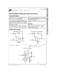
1 A Ultralow Offset Voltage Operational Amplifiers OP07. FEATURES PIN CONNECTIONS. Low VOS: 75 V Max Epoxy Mini-Dip (P-Suffix). Low VOS Drift: V/ C Max 8-Pin SO (S-Suffix). Ultra-Stable vs. Time: V/Month Max Low Noise: V p-p Max Wide Input Voltage Range: 14 V VOS TRIM 1 8 VOS TRIM. OP07. Wide Supply Voltage Range: 3 V to 18 V IN 2 7 V+. Fits 725,108A/308A, 741, AD510 Sockets +IN 3 6 OUT. 125 C Temperature-Tested Dice V 4 5 NC. NC = NO CONNECT. APPLICATIONS. Wireless Base Station Control Circuits Optical Network Control Circuits Instrumentation Sensors and Controls Thermocouples RTDs Strain Bridges Shunt Current Measurements high closed-loop gains. Stability of offsets and gain with time or Precision Filters variations in temperature is excellent. The accuracy and stability GENERAL DESCRIPTION of the OP07, even at high gain, combined with the freedom The OP07 has very low input Offset Voltage (75 V max for from external nulling have made the OP07 an industry standard OP07E) which is obtained by trimming at the wafer stage.
2 These for instrumentation applications. low Offset voltages generally eliminate any need for external null- The OP07 is available in two standard performance grades. The ing. The OP07 also features low input bias current ( 4 nA for OP07E is specified for operation over the 0 C to 70 C range, and OP07E) and high open-loop gain (200 V/mV for OP07E). The OP07C over the 40 C to +85 C temperature range. low offsets and high open-loop gain make the OP07 particularly The OP07 is available in epoxy 8-lead Mini-DIP and 8-lead SOIC. useful for high-gain instrumentation applications. It is a direct replacement for 725,108A, and OP05 Amplifiers ;. The wide input Voltage range of 13 V minimum combined with 741-types may be directly replaced by removing the 741's nulling high CMRR of 106 dB (OP07E) and high input impedace pro- potentiometer.
3 For improved specifications, see the OP177 or vides high accuracy in the noninverting circuit configuration. OP1177. For ceramic DIP and TO-99 packages and standard Excellent linearity and gain accuracy can be maintained even at micro circuit (SMD) versions, see the OP77. Figure 1. Simplified Schematic REV. A. Information furnished by Analog Devices is believed to be accurate and reliable. However, no responsibility is assumed by Analog Devices for its use, nor for any infringements of patents or other rights of third parties that One Technology Way, Box 9106, Norwood, MA 02062-9106, may result from its use. No license is granted by implication or otherwise Tel: 781/329-4700 under any patent or patent rights of Analog Devices. Fax: 781/326-8703 Analog Devices, Inc., 2002. OP07 SPECIFICATIONS.
4 OP07E electrical CHARACTERISTICS (V = 15 V, T = 25 C, unless otherwise noted.)S A. Parameter Symbol Conditions Min Typ Max Unit INPUT CHARACTERISTICS. Input Offset Voltage1 VOS 30 75 V. Long-Term VOS Stability2 VOS/Time V/Mo Input Offset Current IOS nA. Input Bias Current IB nA. Input Noise Voltage en p-p Hz to 10 Hz3 V p-p Input Noise Voltage Density en fO = 10 Hz nV Hz fO = 100 Hz3 nV Hz fO = 1 kHz nV Hz Input Noise Current In p-p 14 30 pA p-p Input Noise Current Density In fO = 10 Hz pA Hz fO = 100 Hz3 pA Hz fO = 1 kHz pA Hz Input Resistance Differential Mode4 RIN 15 50 m . Input Resistance Common-Mode RINCM 160 G . Input Voltage Range IVR 13 14 V. Common-Mode Rejection Ratio CMRR VCM = 13 V 106 123 dB. Power Supply Rejection Ratio PSRR VS = 3 V to 18 V 5 20 V/V. Large-Signal Voltage Gain AVO RL 2 k , VO = 10 V 200 500 V/mV.
5 RL 500 , VO = V, V S = 3 V4 150 400 V/mV. OUTPUT CHARACTERISTICS. Output Voltage Swing VO RL 10 k V. RL 2 k V. RL 1 k V. DYNAMIC PERFORMANCE. Slew Rate SR RL 2 k 3 V/ s Closed-Loop Bandwidth BW AVOL = 15 MHz Closed-Loop Output Resistance RO VO = 0, IO = 0 60 . Power Consumption Pd VS = 15 V, No Load 75 120 mW. VS = 13 V, No Load 4 6 mW. Offset Adjustment Range RP = 20 k 4 mV. NOTES. 1. Input Offset Voltage measurements are performed by automated test equipment approximately seconds after application of power. 2. Long-term input Offset Voltage stability refers to the averaged trend time of VOS vs. Time over extended periods after the first 30 days of operation. Excluding the ini- tial hour of operation, changes in VOS during the first 30 operating days are typically V refer to the typical performance curves.
6 Parameter is sample tested. 3. Sample tested. 4. Guaranteed by design. 5. Guaranteed but not tested. Specifications subject to change without notice. 2 REV. A. OP07. OP07C electrical CHARACTERISTICS (V = 15 V, T = 25 C, unless otherwise noted.) S A. Parameter Symbol Conditions Min Typ Max Unit INPUT CHARACTERISTICS. Input Offset Voltage1 VOS 60 150 V. Long-Term VOS Stability2 VOS/Time V/Mo Input Offset Current IOS nA. Input Bias Current IB nA. Input Noise Voltage en p-p Hz to 10 Hz3 V p-p Input Noise Voltage Density en fO = 10 Hz nV Hz fO = 100 Hz3 nV Hz fO = 1 kHz nV Hz Input Noise Current In p-p 15 35 pA p-p Input Noise Current Density In fO = 10 Hz pA Hz fO = 100 Hz3 pA Hz fO = 1 kHz pA Hz Input Resistance- Differential Mode4 RIN 8 33 m . Input Resistance- Common-Mode RINCM 120 G.
7 Input Voltage Range IVR 13 14 V. Common-Mode Rejection Ratio CMRR VCM = 13 V 100 120 dB. Power Supply Rejection Ratio PSRR VS = 3 V to 18 V 7 32 V/V. Large-Signal Voltage Gain AVO RL 2 k , VO = 10 V 120 400 V/mV. RL 500 , VO = V, V S = 3 V4 100 400 V/mV. OUTPUT CHARACTERISTICS. Output Voltage Swing VO RL 10 k V. RL 2 k V. RL 1 k V. DYNAMIC PERFORMANCE. Slew Rate SR RL 2 k 3 V/ s Closed-Loop Bandwidth BW AVOL = 15 MHz Closed-Loop Output Resistance RO VO = 0, IO = 0 60 . Power Consumption Pd VS = 15 V, No Load 80 150 mW. VS = 13 V, No Load 4 8 mW. Offset Adjustment Range RP = 20 k 4 mV. NOTES. 1. Input Offset Voltage measurements are performed by automated test equipment approximately seconds after application of power. 2. Long-term input Offset Voltage stability refers to the averaged trend time of VOS vs.
8 Time over extended periods after the first 30 days of operation. Excluding the ini- tial hour of operation, changes in VOS during the first 30 operating days are typically V refer to the typical performance curves. Parameter is sample tested. 3. Sample tested. 4. Guaranteed by design. 5. Guaranteed but not tested. Specifications subject to change without notice. REV. A 3 . OP07 SPECIFICATIONS. OP07E electrical CHARACTERISTICS (V = 15 V, 0 C T 70 C, unless otherwise noted.). S A. Parameter Symbol Conditions Min Typ Max Unit INPUT CHARACTERISTICS. Input Offset Voltage1 VOS 45 130 V. Voltage Drift without External Trim2 TCVOS V/ C. Voltage Drift with External Trim3 TCVOSN RP = 20 k V/ C. Input Offset Current IOS nA. Input Offset Current Drift TCIOS 8 35 pA/ C. Input Bias Current IB nA.
9 Input Bias Current Drift TCIB 13 35 pA/ C. Input Voltage Range IVR 13 V. Common-Mode Rejection Ratio CMRR VCM = 13 V 103 123 dB. Power Supply Rejection Ratio PSRR VS = 3 V to 18 V 7 32 V/V. Large-Signal Voltage Gain AVO RL 2 k , VO = 10 V 180 450 V/mV. OUTPUT CHARACTERISTICS. Output Voltage Swing VO RL 10 k 12 V. NOTES. 1. Input Offset Voltage measurements are performed by automated test equipment approximately seconds after application of power. 2. Guaranteed by design. 3. Sample tested. Specifications subject to change without notice. (VS = 15 V, 40 C TA 85 C, unless otherwise noted.). OP07C electrical CHARACTERISTICS. Parameter Symbol Conditions Min Typ Max Unit INPUT CHARACTERISTICS. Input Offset Voltage1 VOS 85 250 V. Voltage Drift without External Trim2 TCVOS V/ C. Voltage Drift with External Trim3 TCVOSN RP = 20 k V/ C.
10 Input Offset Current IOS nA. Input Offset Current Drift TCIOS 12 50 pA/ C. Input Bias Current IB nA. Input Bias Current Drift TCIB 18 50 pA/ C. Input Voltage Range IVR 13 V. Common-Mode Rejection Ratio CMRR VCM = 13 V 97 120 dB. Power Supply Rejection Ratio PSRR VS = 3 V to 18 V 10 51 V/V. Large-Signal Voltage Gain AVO RL 2 k , VO = 10 V 100 400 V/mV. OUTPUT CHARACTERISTICS. Output Voltage Swing VO RL 10 k 11 V. NOTES. 1. Input Offset Voltage measurements are performed by automated test equipment approximately seconds after application of power. 2. Guaranteed by design. 3. Sample tested. Specifications subject to change without notice. 4 REV. A. OP07. ABSOLUTE MAXIMUM RATINGS* Package Type JA* JC Units Supply Voltage (VS) .. 22 V. Input Voltage * .. 22 V 8-Lead Plastic DIP (P) 103 43 C/W.