
GENERAL DESCRIPTION
when designing PCB’s which may be subject to high levels of board flexure. APPLICATIONS High Flexure Stress Circuit Boards • e.g. Depanelization: Components near edges of board. Variable Temperature Applications • Soft termination offers improved reliability performance in applications where there is temperature variation. • e.g.
Download GENERAL DESCRIPTION

Information
Domain:
Source:
Link to this page:
Documents from same domain
RF/Microwave Capacitors
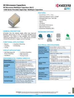
datasheets.kyocera-avx.comRF/Microwave Capacitors 100B Series Porcelain Superchip® Multilayer Capacitors RF/Microwave Multilayer Capacitors (MLC) GENERAL DESCRIPTION KYOCERA AVX, the industry leader, offers new improved ESR/ESL performance for the 100 B Series RF/Microwave Capacitors. This Series is now available with extended operating temperatures up to 175°C.

RADIAL LEADS - datasheets.kyocera-avx.com
datasheets.kyocera-avx.comNPO typical characteristics, see the KYOCERA AVX Multilayer Ceramic Leaded Capacitors Catalog. STYLE* MAXIMUM CAPACITANCE VALUE C0G (NP0) X7R SR29 900 pF .015 μF SR20 1800 pF .033 μF SR28 SR59 900 pF .015 μF SR13 SR21 1800 pF .033 μF SR30 SR61 SR65 7200 pF .12 μF SR40 SR75.015 μF .27 μF SR22 1800 pF .033 μF SR27 1800 pF .033 …

TAJ – Standard & Low Profile TAJ Series
datasheets.kyocera-avx.com• Entertainment / Infotainment Systems • Height Restricted Design STANDARD CASE DIMENSIONS: millimeters (inches) LOW PROFILE CASE DIMENSIONS: millimeters (inches) XXXXX 227 A LOGO Capacitance Value in pF 227 = 220µF Rated Voltage Code A = 10V ID Code Polarity Band (Anode+) J 1 0 6 Capacitance Value in pF 106 = 10µF Rated Voltage Code …

Automotive MLCC - datasheets.kyocera-avx.com
datasheets.kyocera-avx.com56 Automotive MLCC-NP0 Capacitance Range SIZE 0402 0603 0805 1206 Soldering Reflow/Wave Reflow/Wave Reflow/Wave Reflow/Wave WVDC 25V 50V 25V 50V 100V 200V 25V 50V 100V 200V 250V 25V 50V 100V 200V 250V 500V

PART NUMBER (SEE PAGE 4 FOR COMPLETE PART NUMBER …
datasheets.kyocera-avx.comX7R formulations are called “temperature stable” ceramics and fall into EIA Class II materials. X7R is the most popular of these intermediate dielectric constant materials. Its temperature variation of capacitance is within ±15% from -55°C to +125°C. This capacitance change is …

Low ESR Resin Molded Solid Tantalum Chip, J-Lead TPS ...
datasheets.kyocera-avx.comLow ESR Resin Molded Solid Tantalum Chip, J-Lead Low ESR TPS Series – Standard & Low Profile FEATURES • Low ESR Series of Robust Mn0 2 Solid Electrolyte Capacitors • 100% Surge Current Tested • CV Range: 0.15-1500μF / 2.5-50V • 14 Case Sizes Available • Power Supply Applications APPLICATIONS • General Medium Power DC/DC Convertors
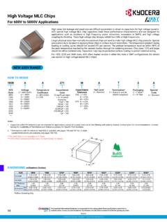
High Voltage MLC Chips
datasheets.kyocera-avx.com95 High Voltage MLC Chips For 600V to 5000V Applications Case Size 0805 1206 1210 1808 1812 Soldering Reflow/Wave Reflow/Wave Reflow Only Reflow Only Reflow Only (L) Length mm 2.10 ± 0.20 3.30 + 0.30 3.30 + 0.40 4.60 + 0.50 4.60 + 0.50

SECTION 2: SOLID CONDUCTIVE POLYMER ELECTROLYTIC …
datasheets.kyocera-avx.comtcj series section 2: solid conductive polymer ... tcjb107m002#0055e b 100 2.5 125 25 6 55 1500 1100 700 400 0 3 tcjb107m002#0070e b 100 2.5 125 25 6 70 1300 900 600 300 1 3 tcjb157m002#0070e b 150 2.5 105 37.5 6 70 1300 900 600 – 3 3 tcjb227m002#0035e b 220 2.5 105 55 8 35 1900 1300 900 – 3 3
Related documents
Designing PCB LPs - wa5vjb.com
www.wa5vjb.comDesigning PCB Log Periodic Antennas Kent Britain WA5VJB Over the last few years, I have developed many PCB Log Periodic antennas from 400 MHz to 11 GHz. I wish I could say I have a secret design process, but there were many variations and small pieces of metal tape on the early models. And while there are software programs such as IE3D and HFSS

PCB Design Tutorial - AlternateZone.com
alternatezone.comnice Printed Circuit Board (PCB) design. For some designers, the PCB design will be a natural and easy extension of the design process. But for many others the process of designing and laying out a PCB can be a very daunting task. There are even very experienced circuit designers who know very little about PCB design,

Layout Design Guide - Toradex
docs.toradex.comstart designing a carrier board. Please use this document together with the design guide of the appropriate Toradex computer module family and the datasheet of the module. 1.2 Additional Documents 1.2.1 Apalis Carrier Board Design Guide This document provides additional information to the schematic design of a carrier board for the Apalis modules.

RNCP Series Stackpole Electronics, Inc.
seielect.comMounted 2 pieces on 1 PCB. MIL-STD-202 Method 108 245 ± 5ºC solder, 2 ± 0.5 seconds. dwell Solder: Sn 96.5 / Ag 3.0 / Cu 0.5. Resistance to Soldering Heat MIL-STD-202 Method 210) - Moisture Resistance
High-Speed Layout Guidelines for Signal Conditioners and ...
www.ti.comPCB manufacturing, layout, and design. 1.2 Critical Signals A primary concern when designing a system is accommodating and isolating high-speed signals. As high-speed signals are most likely to impact or be impacted by other signals, they must be laid out early
Chiplets and Heterogeneous Packaging Are Changing System ...
www.cadence.comChiplets and Heterogeneous Packaging Are Changing System Design and Analysis www.cadence.com 4 f High-performance 3D die stacking techniques for better integration with the chip system and power/performance integration f Accelerated speed f Lower development cost offered by modular integration f Lower manufacturing costs by purchasing known-good die …

VRF SYSTEMS
lghvac.com• Advanced PCB Cooling. Improved cooling performance of the inverter . PCB by using liquid refrigerant instead of heat . sink cooling methods. • LG Inverter Scroll. Innovative high side-shell design creates a more . compact unit providing the same capacity output, with greater reliability in cold climates. • HiPOR™ (High-Pressure Oil ...

Designing a PCB - Stanford University
web.stanford.eduDesigning a PCB • Design the schematic • Select the components • Place components on PCB • Route signals and power planes • Send design to manufacturer • Assemble

Design Guide and Example of Stencil for Exposed Pad
fscdn.rohm.comPCB Cu Package Figure 1. Presence of standoff with gull wing package Stencil for flat lead package ... conditions must be taken into account when designing circuits for mass production. The technical information specified herein is intended only to show the typical functions of and

The EAGLE Schematic & PCB Layout Editor - A Guide
intranet.ee.ic.ac.ukThis guide assumes that you are designing a two-sided PCB with plated-through holes (PTH), the normal case, and supported by the freeware version of EAGLE providing your board is no larger than 100mmX80mm. If you want to download the freeware EAGLE to your own PC this is easy. Look for the latest freeware version for your operating system ...