
I2S bus specification - SparkFun Electronics
of n” decoder, the MSB latch (B1) is enabled (EN1 = 1), and the first serial data bit (the MSB) is latched into B1 on the rising edge of SCK. As the counter increases by one every clock pulse, subsequent data bits are latched into B2 to Bn. On the next …
Download I2S bus specification - SparkFun Electronics

Information
Domain:
Source:
Link to this page:
Documents from same domain
AT Commands Reference Guide - SparkFun …
www.sparkfun.comAT Commands Reference Guide 80000ST10025a Rev. 0 - 04/08/06 Reproduction forbidden without Telit Communications S.p.A. written authorization - All …
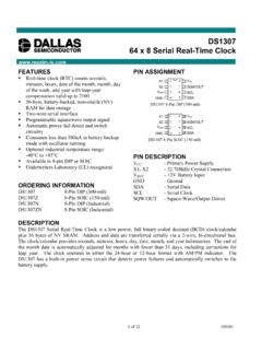
DS1307 64 x 8 Serial Real-Time Clock
www.sparkfun.com1 of 12 100101 FEATURES Real-time clock (RTC) counts seconds, minutes, hours, date of the month, month, day of the week, and year with …

Advanced User Manual - SparkFun Electronics
www.sparkfun.comusage information and a summary of common commands refer to the Install Guide for a given product. Version 4.77 August 27, 2009 Roving Networks reserves the right to make corrections, modifications, and changes to its products, documentation and services ... Advanced User Manual.

Preliminary Product Specification v1 - SparkFun Electronics
www.sparkfun.comRevision 1.0 Page 3 of 75 nRF24L01+ Preliminary Product Specification Writing Conventions This product specification follows a set of typographic rules that make s the document consistent and easy

Single chip 2.4 GHz Transceiver nRF24L01
www.sparkfun.comPRELIMINARY PRODUCT SPECIFICATION nRF24L01 Single Chip 2.4 GHz Radio Transceiver Nordic Semiconductor ASA - Vestre Rosten 81, N-7075 Tiller, Norway - Phone +4772898900 - …
XBee /XBee-PRO RF Modules - SparkFun Electronics
www.sparkfun.comThe XBee®/XBee-PRO® RF Module was designed to mount into a receptacle (socket) and there-fore does not require any soldering when mounting it to a board. The XBee Development Kits con-tain RS-232 and USB interface boards which use two 20-pin receptacles to receive modules.

GSM/GPRS Module - SparkFun Electronics
www.sparkfun.comThis document gives an overview of the LinkSprite GSM/GPRS module: a miniature, single-side board, quad-band GSM 850/EGSM 900/DCS 1800/PCS 1900 module, ready for integration in various kinds of Fix wireless phones and other wireless devices.

16-Channel Constant-Current LED Driver
www.sparkfun.comA6282 Description The A6282 device is designed for LED display applications. This CMOS device includes an input shift register, accompanying data latches, and 16 MOS constant current sink drivers.

+3.3V Low Power Half-Duplex RS-485 Transceivers with ...
www.sparkfun.com10/15/02 SP3481/3485 Low Power Half-Duplex RS485 Transceivers © Copyright 2000 Sipex Corporation 2 SPECIFICATIONS T AMB = T MIN to T MAX and V CC = +3.3V ± 5% ...
XBee /XBee-PRO RF Modules - SparkFun Electronics
www.sparkfun.comDigi International Inc. 11001 Bren Road East Minnetonka, MN 55343 877 912-3444 or 952 912-3444 http://www.digi.com XBee®/XBee-PRO® RF Modules XBee®/XBee-PRO® RF ...
Related documents
Op-Amp/Comparator Application Note
fscdn.rohm.comApplication Note VEE
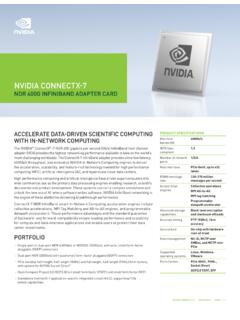
NVIDIA CONNECTX-7 | Datasheet
www.nvidia.comThe last digit of the OPN-suffix displays the default bracket option: B = pull tab, I = internal lock; E = ejector latch. For other bracket types, contact NVIDIA. Note 1.Pre OCP3.2 Spec ADAPTER CARD PORTFOLIO AND ORDERING INFORMATION PCIE STANDUP FORM FACTOR InfiniBand Supported Speeds [Gb/s] Network Ports and Cages Host Interface [PCIe]

Latches, the D Flip-Flop & Counter Design
web.ece.ucsb.eduFebruary 6, 2012 ECE 152A - Digital Design Principles 2 Reading Assignment Brown and Vranesic 7Flip-Flops, Registers, Counters and a Simple Processor 7.1 Basic Latch 7.2 Gated SR Latch 7.2.1 Gated SR Latch with NAND Gates 7.3 Gated D …

PIC16(L)F1508/9 Data Sheet
ww1.microchip.com- AND/OR/XOR/D Flop/D Latch/SR/JK - Inputs from external and internal sources - Output available to pins and peripherals - Operation while in Sleep • Numerically Controlled Oscillator (NCO): - 20-bit accumulator - 16-bit increment - True linear frequency control - High-speed clock input - Selectable Output modes - Fixed Duty Cycle (FDC) mode
PIC16(L)F1934/6/7 Data Sheet
ww1.microchip.com• SR Latch (555 Timer): - Multiple Set/Reset input options - Emulates 555 Timer applications • 2 Comparators: - Rail-to-rail inputs/outputs - Power mode control - Software enable hysteresis • Voltage Reference module: - Fixed Voltage Reference (FVR) with 1.024V, 2.048V and 4.096V output levels - 5-bit rail-to-rail resistive DAC with positive
Chapter 5 Synchronous Sequential Logic
www.cse.iitb.ac.inSR Latch with Control Input! Add an additional control input to determine when the state of the latch can be changed! C=0: S and R are disabled (no change at outputs)! C=1: S and R are active-high 5-12 D Latch! D latch has only two inputs: D(data) and C(control)! Use the value of D to set the output value! Eliminate the indeterminate state in ...
NCS20071 - Operational Amplifier, Rail-to-Rail Output, 3 ...
www.onsemi.comLatch−Up Current (Note 6) ILU 100 mA Moisture Sensitivity Level (Note 7) MSL Level 1 Stresses exceeding those listed in the Maximum Ratings table may damage the device. If any of these limits are exceeded, device functionality should not be assumed, damage may occur and reliability may be affected. 1.