
Quartus Prime - よく使用するピン・オプションの設定方法
Stratix V、Stratix IV、Arria 10、Arria V、Arria II、Cyclone V、Cyclone IV、MAX 10、MAX V、MAX II ※ Quartus Prime 15.1 でサポートしているすべてのデバイス 設定手順 ① Pin Planner を起動します。(Assignments メニュー ⇒ Pin Planner をクリック) ② Pin Planner 内の All Pins リストの目的 ...
Download Quartus Prime - よく使用するピン・オプションの設定方法

Information
Domain:
Source:
Link to this page:
Documents from same domain

Lattice-XO2基板設計時資料
www.macnica.co.jp値を推奨します(lvcmos, lvttl など)。 内部処理が無い専用ピンにつける外部処理の抵抗値としては2.2k - 4.7kΩを推奨します。 或いはフェールセーフ的な観点や設計要件によって、内部プル処理と じレベルで外部プル処 理を行う場合も様です。

Quartus® Prime はじめてガイド
www.macnica.co.jp5. Family, Device & Board Settings ページでは、使用する開発キットに搭載されているインテル FPGA の型 番を選択します。 Family, Device & Board Settings ページ Board Device Family Package Pin count Core speed grade Available devices MAX fi10 FPGA Evaluation Kit MAX 10 EQFP 144 8 10M08SAE144C8G

ModelSim-Altera Edition インストール & ライセンス セット …
www.macnica.co.jpModelSim には複数のエディションがあります。各エディションはそれぞれ使用できる機能や対応言語、シ ミュレーション速度が異なります。ModelSim-Altera Edition およびModelSim-Altera Starter Edition はアルテ ラ社デバイスのシミュレーションに特化したシミュレータ ...

Quartus Prime - EDA ツールの設定方法
www.macnica.co.jpQuartus Prime 開発ソフトウェアは、様々な EDA ツールとインタフェースを取ることができます。論理合成ツー ルから生成された .edif や .vqm ファイルを Quartus Prime 開発ソフトウェアでコンパイルするときや配置配線終

Quartus® Prime はじめてガイド - TimeQuest によるタイミ …
www.macnica.co.jpQuartus® Prime はじめてガイド - TimeQuest によるタイミング制約の方法 Ver.17 / Rev. 2 2018年3月 3/32 ALTIMA ompany, MANIA, Inc. / ELSENA,Inc. はじめに この「Quartus® はじめてガイド」シリーズは、インテル® Quartus® Prime / Quartus® II 開発ソフトウェアを使用する
Quartus® Prime はじめてガイド
www.macnica.co.jpQuartus Prime はじめてガイド – Signal Tap ロジック・アナライザの使い方 Ver.17.1 / Rev. 1 2018 年1 月 8/28 ALTIMA Company, MACNICA, Inc. / ELSENA,Inc. 6 つのペインで構成された STP ファイルが表示されます。 Instance Manager ペインに auto_signaltap_0 という名称の Signal Tap IP の ...

Quartus Prime はじめてガイド - ピン・アサインの方法
www.macnica.co.jpALTIMA Corp. ELSENA,Inc. Quartus Prime はじめてガイド ピン・アサインの方法 ver.15.1 2016 年2 月 Rev.1

JTAG基板設計資料 - 株式会社マクニカ
www.macnica.co.jpJTAG_Board_Design_Rev1.1.ppt Page: 3 Dec 2008 ・本資料はJTAGを使用した書き込みの方法、注意点などをまとめた基 板設計資料です。
Related documents

Stratix 5700 - Rockwell Automation
literature.rockwellautomation.comV +-Mod 5500S2 Stratix 5700 with NAT with NAT Device Level Ring Technology The Device Level Ring (DLR) protocol is used for high-speed, high-performance Superapplications where resiliency is required. DLR is a layer 2 protocol that allows multi-port EtherNet/IP devices to form a …
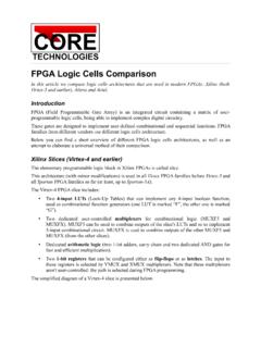
FPGA Logic Cells Comparison - Sharif
ee.sharif.eduAltera FPGAs (Stratix and Cyclone families) uses slightly different logic blocks called “Adaptive Logic Modules” (ALMs). ALM resources include: • Two 4-input LUTs and four 3-input LUTs for combinational logic implementation. Fig. 2: A simplified diagram of a Virtex-5 FPGA slice LUT LUT LUT LUT Arithmetic and carry logic D CLK CE SR D CLK ...
Stratix Industrial Networks Infrastructure At-A-Glance ...
literature.rockwellautomation.comStratix Industrial Networks Infrastructure At-A-Glance Switching and Routing Security Appliance 1783-NATR Network Address Translation Router Stratix® 2000 ... 12 V/24V/48V DC Class 2 / SELV 12V/24V/48V DC Class 2 / SELV 12V-54V DC 12V-48V DC or 12V-54V DC 24V-60V DC or 100-240V DC and 100-250V DC Maximum operating range: 9.6 to 60 VDC

Practical introduction to PCI Express with FPGAs
indico.cern.cho Stratix GX, Stratix II GX, and Arria GX support o No S4GX, C4GX and A2GX Hard IP support • EZDMA2 Altera/Xilinx o Support Hard IP inside Altera: Cyclone IV GX, Arria II GX, and Stratix IV GX o Hard IP inside Xilinx: Virtex-5/6, Spartan-6 o Same user/DMA interface as XpressLite
Allen-Bradley PowerFlex 525 AC Drives
www.infoplc.netV/Hz Sensorless vector control Economizer mode Closed Loop Velocity Vector Control Permanent magnet motor control (future firmware release Dec 2013) Positioning with closed loop feedback allows simple positioning 10

Intel FPGA Download Cable II User Guide
www.intel.comMAX 10 As specified by VCCIO Stratix II, Stratix II GX As specified by VCCSEL Stratix III, Stratix IV As specified by VCCPGM or VCCPD Stratix V As specified by VCCPD Bank 3A 2.2. Cable-to-Board Connection A standard USB cable connects to the USB port on the device. UG-01150 | 2018.04.19
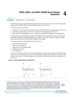
DDR2, DDR3, and DDR4 SDRAM Board Design Guidelines 4
www.intel.co.jpStratix IV Leveling Stratix V Leveling Arria 10 Leveling RelatedInformation www.JEDEC.org Read and Write Leveling A major difference between DDR2 and DDR3/DDR4 SDRAM is the use of leveling. To improve signal integrity and support higher frequency operations, the JEDEC committee defined a fly-by termination

Stratix Ethernet Switch Specifications
www.ideadigitalcontent.comCorrections to Stratix 5700 alarm relay ratings and power supply requirements 3 Addition of Stratix 8000 and Stratix 8300 expansion modules (cat. nos. 1783-MX04S, 1783-MX08S) 8 Addition of Stratix 2000 switch (cat. no. 1783-US8T) 22 Cat. No. Total Ports RJ45 Ports(1) (1) FE = Fast Ethernet; GE = Gigabit Ethernet.
Understanding and Meeting FPGA Power Requirements White …
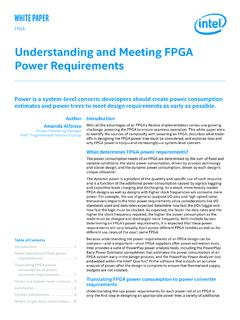
www.intel.com1 Example V CC core voltage power supply operating conditions for the Stratix V FPGA, as shown in Table 6 of the Stratix V data sheet. In this example, the Stratix V core input must be supplied with either 0.9 V or 0.85 V, depending on the speed grade variant, with ±30 mV allowable steady-state DC voltage tolerance.